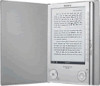
Sony PRS-505/SC Service Manual - Page 40
Main Board, Ic1001, Mc9328mxlvp20r2, Main Cpu
 |
View all Sony PRS-505/SC manuals
Add to My Manuals
Save this manual to your list of manuals |
Page 40 highlights
PRS-505 MAIN BOARD IC1001 MC9328MXLVP20R2 (MAIN CPU) Pin No. Pin Name I/O Description A1 AUDIO3_DATA O Serial data output to the audio D/A converter A2 SRAMINT I Not used A3 VBUS I VBUS input from the USB connector A4 XUSBD_OE O USB output enable signal output terminal Not used A5 USBD_SUSPND O USB suspend signal output terminal Not used A6 USB_VM I USB minus input terminal Not used A7 USB20INT I Interrupt signal input from the USB controller A8 SSI_TXCLK O Bit clock signal output to the audio D/A converter A9 NAND-CE1 O Chip enable signal output terminal Not used A10 NAND-CE0 O Chip enable signal output to the NAND flash memory A11 ERR O Error signal output to the indicator controller A12 RDY I Ready signal input from the indicator controller A13 to A15 PD2, PD4, PD5 O Video data output to the indicator controller B1 AUDIO1_CS O Chip select signal output to the audio D/A conberter B2 AUDIO2_CLK O Clock signal output to the audio D/A conberter B3 SD_DET I SD memory card detect signal input from the SD memory card slot "L": SD memory card slot in B4 USBD_AFE O USB analog front end enable signal output terminal Not used B5 USBD_RCV I USB serial data input terminal Not used B6 USBD_VMO O USB minus output terminal Not used B7 SSI_RXDAT I Serial data input terminal Not used B8 UART1_TXD O Serial data output to the sub CPU B9 RY/#BY I Ready/busy select signal input from the NAND flash memory and NOR flash memory B10 PCLK O Pixel clock signal output to the indicator controller B11 STBY O Standby signal output to the indicator controller B12 to B15 PD0, PD3, PD6, PD7 O Video data output to the indicator controller C1 D31 I/O Two-way data bus with the SD-RAM C2 USBLED O LED drive signal output terminal for USB indicator "H": LED on C3 MSINT I Not used C4 SD_WP I SD memory card write protect switch signal input from the SD memory card slot C5 PCAUDIO O Power supply on/off signal output terminal "H": power on C6 USBD_VPO O USB plus output terminal Not used C7 UART2_RXD I Serial data input terminal Not used C8 SSI_TXFS O L/R sampling clock signal output to the audio D/A converter C9 UART1_RTS I Request to send signal input from the sub CPU C10 SRA3P O Reset signal output to the indicator controller C11 FCLK O Frame clock signal output to the indicator controller C12 to C14 PD8, PD9, PD12 O Video data output to the indicator controller C15 NVDD2 - Power supply terminal (+2.9V) D1 A23 O Address signal output to the address decoder D2 A24 O Address signal output terminal Not used D3 PCR5CCLK O Host clock control signal output terminal D4 PB17 O Not used D5 NVDD1 - Power supply terminal (+2.9V) D6 USBD_VP I USB plus input terminal Not used D7 QVDD4 - Power supply terminal (+1.9V) D8 UART2_TXD O Serial data output terminal Not used D9 NVDD3 - Power supply terminal (+2.9V) D10 NAND-ALE O Address latch enable signal output to the NAND flash mamory D11 LCLK O Latch clock signal output to the indicator controller D12, D13 PD1, PD11 O Video data output to the indicator controller D14 HPSET I Not used D15 PD13 O Video data output to the indicator controller E1, E2 A21, A22 O Address signal output to the address decoder E3, E4 D30, D29 I/O Two-way data bus with the SD-RAM E5 NVDD1 - Power supply terminal (+2.9V) E6 VSS - Ground terminal E7 PCSDCARD O Regulator control signal output terminal 40
-
 1
1 -
2
-
3
-
4
-
5
-
6
-
7
-
8
-
9
-
10
-
11
-
12
-
13
-
14
-
15
-
16
-
17
-
18
-
19
-
20
-
21
-
22
-
23
-
24
-
25
-
26
-
27
-
28
-
29
-
30
-
31
-
32
-
33
-
34
-
 35
35 -
 36
36 -
 37
37 -
 38
38 -
 39
39 -
 40
40 -
 41
41 -
 42
42 -
 43
43 -
 44
44 -
 45
45 -
46
-
47
-
48
-
49
-
50
-
51
-
52
-
53
-
54
-
55
-
56
-
57
-
58
-
59
-
60
-
61
-
62
-
63
-
64
-
65
-
66
-
67
-
68
-
69
-
70
-
71
-
72
-
73
-
74
 |
 |
