Sony PRS-505/SC Service Manual - Page 36
Main Board, Ic301, A3p125-vqg100, Indicator Controller - video
 |
View all Sony PRS-505/SC manuals
Add to My Manuals
Save this manual to your list of manuals |
Page 36 highlights
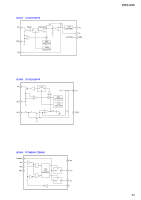
PRS-505 MAIN BOARD IC301 A3P125-VQG100 (INDICATOR CONTROLLER) Pin No. Pin Name I/O Description 1 GND - Ground terminal 2 to 8 PD15 to PD9 I Video data input from the main CPU 9 GND - Ground terminal 10, 11 PD8, PD7 I Video data input from the main CPU 12 GND - Ground terminal 13 PD6 I Video data input from the main CPU 14 GND - Ground terminal 15, 16 PD5, PD4 I Video data input from the main CPU 17 VCC - Power supply terminal (+1.5V) 18 VCCI - Power supply terminal (+3.3V) 19 to 22 PD3 to PD0 I Video data input from the main CPU 23 PSFL I Not used 24 VMV - Power supply terminal (+3.3V) 25 GND - Ground terminal 26 FCLK I Frame clock signal input from the main CPU 27 LCLK I Latch clock signal input from main CPU 28 PCLK I Pixel clock signal input from the main CPU 29 SDLE O Latch enable signal output to the ink indicator element 30 to 36 SDDO0 to SDDO6 O Video data input from the main CPU 37 VCC - Power supply terminal (+1.5V) 38 GND - Ground terminal 39 VCC1 - Power supply terminal (+3.3V) 40 SDDO7 O Video data input from the main CPU 41 SDCLK O Clock signal output to the ink indicator element 42 SDOE O Output enable signl output to the ink indicator element 43 GDOE O Output enable signal output to the ink indicator element 44 GDSP O Sharp panel signal output to the ink indicator element 45 GDCLK O Clock signal output to the ink indicator element 46 GND - Ground terminal 47 TCK - Not used 48 TDI - Not used 49 TMS - Not used 50 VMV - Power supply terminal (+3.3V) 51 GND - Ground terminal 52 VPUMP - Not used 53 NC - Not used 54 TDO - Not used 55 TRST - Not used 56 VJTAG - Not used 57 to 59 SDCE5 to SDCE3 O Chip enable signal output terminal Not used 60 to 62 SDCE2 to SDCE0 O Chip enable signal output to the ink indicator element 63 SDSHR O Not used 64 GDRL O Not used 65 PWRCOM O Command signal output to the VCOM switch 66 VCCI - Power supply terminal (+3.3V) 67 GND - Ground terminal 68 VCC - Power supply terminal (+1.5V) 69 PWR2 O Power supply control signal output terminal 70 BDR1 O Border control signal output terminal 71 BDR0 O Border control signal output terminal 72 PWR0 O Power supply control signal output terminal 73 PWR1 O Power supply control signal output terminal 74 VMV - Power supply terminal (+3.3V) 75 GND - Ground terminal 76 SPIDO O Not used 77 SPICLK O Not used 78 SPIDI I Not used 79 SPICS O Not used 36
-
 1
1 -
2
-
3
-
4
-
5
-
6
-
7
-
8
-
9
-
10
-
11
-
12
-
13
-
14
-
15
-
16
-
17
-
18
-
19
-
20
-
21
-
22
-
23
-
24
-
25
-
26
-
27
-
28
-
29
-
30
-
 31
31 -
 32
32 -
 33
33 -
 34
34 -
 35
35 -
 36
36 -
 37
37 -
 38
38 -
 39
39 -
 40
40 -
 41
41 -
42
-
43
-
44
-
45
-
46
-
47
-
48
-
49
-
50
-
51
-
52
-
53
-
54
-
55
-
56
-
57
-
58
-
59
-
60
-
61
-
62
-
63
-
64
-
65
-
66
-
67
-
68
-
69
-
70
-
71
-
72
-
73
-
74
 |
 |
