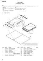
Sony PRS-505/SC Service Manual - Page 41
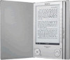
Sony PRS-505/SC - Portable Reader System Manual
 |
View all Sony PRS-505/SC manuals
Add to My Manuals
Save this manual to your list of manuals |
Page 41 highlights
PRS-505 Pin No. E8 E9 E10 E11 E12 E13 E14 E15 F1, F2 F3, F4 F5, F6 F7 F8 F9 F10 F11 F12, F13 F14 F15 G1, G2 G3, G4 G5 G6 G7 G8 to G10 G11 G12 G13 G14 G15 H1 H2 H3 to H5 H6 to H9 H10 H11 H12 H13 H14 H15 J1, J2 J3, J4 J5 J6, J7 J8 J9 J10 J11 J12 J13 J14, J15 K1 K2 K3 K4 Pin Name UART1_RXD UART1_CTS NAND-CLE PDOE PD10 TIN PCA3PCORE SRETHER A20, A19 D28, D27 NVDD1 PCMSCARD SRUSB20 SSI_TXDAT SRSRAM1 QVDD3 PD14, PD15 USB_CHRG SRDSP A17, A18 D26, D25 NVDD1 VSS NVDD4 VSS PCA3PIO PCUSB11 RSCINT MSDET SRMS A15 A16 D22 to D24 VSS NVDD2 USB_BOOT PCR5C PA14 I2CSDA TMS A14, A12 D21, D20 NVDD1 VSS QVDD1 VSS SRR5C I2CSCL TCK XTDO BOOT1, BOOT0 A13 A11 XCS2 D19 I/O Description I Serial data input from the sub CPU O Clear to send signal output to the sub CPU O Command latch enable signal output to the NAND flash mamory O Output enable signal output to the indicator controller O Video data output to the indicator controller I Timer input terminal Not used O Regulator control signal output terminal O Not used O Address signal output to the NOR flash memory I/O Two-way data bus with the SD-RAM - Power supply terminal (+2.9V) O Regulator control signal output terminal O No used O Audio data output to the audio D/A converter O Not used - Power supply terminal (+1.9V) O Video data output to the indicator controller O USB charge enable signal output to the sub CPU O Reset signal output to the audio D/A converter O Address signal output to the NOR flash memory I/O Two-way data bus with the SD-RAM - Power supply terminal (+2.9V) - Ground terminal - Power supply terminal (+2.9V) - Ground terminal O Regulator control signal output terminal O Not used I Interrupt request signal input from the memory stick duo/SD memory card controller I Memory stick duo detect signal input from the memory stick duo slot "L": memory stick duo slot in O Not used O Address signal output to the memory stick duo/SD memory card controller, SD-RAM and NOR flash memory O Address signal output to the NOR flash memory I/O Two-way data bus with the SD-RAM - Ground terminal - Power supply terminal (+2.9V) I Main CPU boot mode control signal input from the sub CPU O Hardware suspend mode output to the memory stick duo/SD memory card controller "L": hardware suspend mode O Not used I/O Two-way IIC bus with the temperature sensor I Test mode select signal input terminal Not used O Address signal output to the memory stick duo/SD memory card controller, SD-RAM and NOR flash memory I/O Two-way data bus with the SD-RAM - Power supply terminal (+2.9V) - Ground terminal - Power supply terminal (+1.9V) - Ground terminal O Reset signal output to the memory stick duo/SD memory card controller O IIC bus serial clock signal output to the temperature sensor I Test clock signal input terminal Not used O Test data signal output terminal Not used I System boot mode select signal input terminal O Address signal output to the memory stick duo/SD memory card controller, SD-RAM and NOR flash memory O Address signal output to the memory stick duo/SD memory card controller and NOR flash memory O Chip select signal output to the SD-RAM I/O Two-way data bus with the SD-RAM 41
-
 1
1 -
2
-
3
-
4
-
5
-
6
-
7
-
8
-
9
-
10
-
11
-
12
-
13
-
14
-
15
-
16
-
17
-
18
-
19
-
20
-
21
-
22
-
23
-
24
-
25
-
26
-
27
-
28
-
29
-
30
-
31
-
32
-
33
-
34
-
35
-
 36
36 -
 37
37 -
 38
38 -
 39
39 -
 40
40 -
 41
41 -
 42
42 -
 43
43 -
 44
44 -
 45
45 -
 46
46 -
47
-
48
-
49
-
50
-
51
-
52
-
53
-
54
-
55
-
56
-
57
-
58
-
59
-
60
-
61
-
62
-
63
-
64
-
65
-
66
-
67
-
68
-
69
-
70
-
71
-
72
-
73
-
74
 |
 |
