Sony PRS-505/SC Service Manual - Page 38
Main Board, Ic401, Sn412005rhlr, Charge Control - charge usb
 |
View all Sony PRS-505/SC manuals
Add to My Manuals
Save this manual to your list of manuals |
Page 38 highlights
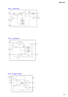
PRS-505 MAIN BOARD IC401 SN412005RHLR (CHARGE CONTROL) Pin No. Pin Name I/O Description 1 LDO O Power supply (+3.3V) output terminal 2 STAT1 O Charge state signal output to the sub CPU and LED drive signal for CHARGE indicator 3 STAT2 O Charge state signal output to the sub CPU 4 AC I Power supply input from the AC adaptor 5, 6 BAT I/O Power supply voltage input from the rechargeable battery or charge voltage output to the rechargeable battery 7 ISET2 I Charge current setting siganal input from the sub CPU "L": 100 mA, "H": 500 mA Fixed at "H" charging voltage in this set 8 PSEL I Charge source selection siganal input terminal "L": USB (pin 20), "H": AC (pin 4) Fixed at "H" charging voltage in this set 9 CE I Chip enable signal input terminal Not used 10 ISET1 O Setting terminal for AC input charge current and AC precharge/termination 11 VSS - Ground terminal 12 TS I Thermal detection signal input terminal 13 DPPM I Setting terminal for the dinamic power pass management 14 TMR I Timer program input terminal (Becomes impossible to do safety timer and charge termination when connecting LOD (pin 1)) 15 to 17 OUT O Power supply voltage output terminal 18 XACPG O External DC power state detection signal output to the sub CPU "L": external DC power on 19 XUSBPG O USB power state detection signal output terminal Not used 20 USB I Charge voltage input terminal from the USB connector 21 GND - Ground terminal 38
-
 1
1 -
2
-
3
-
4
-
5
-
6
-
7
-
8
-
9
-
10
-
11
-
12
-
13
-
14
-
15
-
16
-
17
-
18
-
19
-
20
-
21
-
22
-
23
-
24
-
25
-
26
-
27
-
28
-
29
-
30
-
31
-
32
-
 33
33 -
 34
34 -
 35
35 -
 36
36 -
 37
37 -
 38
38 -
 39
39 -
 40
40 -
 41
41 -
 42
42 -
 43
43 -
44
-
45
-
46
-
47
-
48
-
49
-
50
-
51
-
52
-
53
-
54
-
55
-
56
-
57
-
58
-
59
-
60
-
61
-
62
-
63
-
64
-
65
-
66
-
67
-
68
-
69
-
70
-
71
-
72
-
73
-
74
 |
 |
