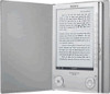
Sony PRS-505/SC Service Manual - Page 39
Main Board, Ic801, Hd64f38004fp10v-v198, Sub Cpu
 |
View all Sony PRS-505/SC manuals
Add to My Manuals
Save this manual to your list of manuals |
Page 39 highlights
PRS-505 MAIN BOARD IC801 HD64F38004FP10V-V198 (SUB CPU) Pin No. Pin Name I/O Description 1 BATT-DC I Power supply input from the AC adaptor 2 X1 I System clock input terminal (32.768 kHz) 3 X2 O System clock output terminal (32.768 kHz) 4 VSS - Ground terminal 5 OSC2 O System clock output terminal (4.9152 MHz) 6 OSC1 I System clock input terminal (4.9152 MHz) 7 TEST I Connect to ground 8 XRESET I System reset signal input terminal "L": reset 9 ISET1 I Charge current setting siganal input terminal 10 ISET2 O Charge current setting siganal output to the charge control 11 to 13 P33 to P35 - Connect to power supply 14, 15 STAT1, STAT2 I Charge state monitor input from the charge control 16 VCC - Power supply terminal (+2.9V) 17 to 19 V1 to V3 - Connect to power supply 20 PWRON O Main power on/off control signal output terminal "H": main power on 21 AD_ON O Rechargeable battery input control signal output terminal "H": rechargeable battery input 22 POR O Power on reset signal output to the main CPU "H": reset 23 XM_RESET O Master reset signal output to the main CPU "L": reset 24 USBON O USB charge on/off control signal output terminal "H": USB charge on 25 to 29 KEY_OUT7 to KEY_OUT3 O Key scan signal output terminal Not used 30 to 32 KEY_OUT2 to KEY_OUT0 O Key scan signal output terminal 33 to 40 KEY_IN7 to KEY_IN0 I Key scan signal input terminal 41 KEY-INT I Key scan interrupt input from the KEY-ON (pin 53) 42 CTS I Clear to send signal input from the main CPU 43 USBDET I USB cable connect signal input terminal "H": USB cable is connected 44 LOW-BATT-LI I Rechargeable battery low detect signal input terminal 45 WKP3 I Not used 46 USBCHG I USB charge enable signal input from the main CPU 47 DCDET I External DC power state detection signal input from the charge control "L": external DC power on 48 STBY_SW I Power switch signal input terminal 49 KEYLED O LED drive signal output terminal Not used 50 LED_1 O LED drive signal output terminal for USB indicator "H": LED on 51 LED_2 O LED drive signal output terminal Not used 52 USBBOOT O Main CPU boot mode control signal output to the main CPU 53 KEY-ON O Key scan interrupt signal output to the KEY-INT (pin 41) 54 P95 O Connect to power supply 55 VSS - Ground terminal 56 IRQAEC I Not used 57 RTS O Request to send signal output to the main CPU 58 RXD I Serial data input from the main CPU 59 TXD O Serial data output to the main CPU 60 IRQ0 I Not used 61 AVCC - Power supply terminal (+2.9V) 62 AN0 I Not used 63 BATT-LI I Rechargeable battery input terminal 64 AN2 I Not used 39
-
 1
1 -
2
-
3
-
4
-
5
-
6
-
7
-
8
-
9
-
10
-
11
-
12
-
13
-
14
-
15
-
16
-
17
-
18
-
19
-
20
-
21
-
22
-
23
-
24
-
25
-
26
-
27
-
28
-
29
-
30
-
31
-
32
-
33
-
 34
34 -
 35
35 -
 36
36 -
 37
37 -
 38
38 -
 39
39 -
 40
40 -
 41
41 -
 42
42 -
 43
43 -
 44
44 -
45
-
46
-
47
-
48
-
49
-
50
-
51
-
52
-
53
-
54
-
55
-
56
-
57
-
58
-
59
-
60
-
61
-
62
-
63
-
64
-
65
-
66
-
67
-
68
-
69
-
70
-
71
-
72
-
73
-
74
 |
 |
