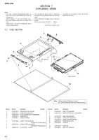
Sony PRS-505/SC Service Manual - Page 43
Sony PRS-505/SC - Portable Reader System Manual
 |
View all Sony PRS-505/SC manuals
Add to My Manuals
Save this manual to your list of manuals |
Page 43 highlights
PRS-505 Pin No. P11 P12 P13 P14 P15 R1 R2 R3 R4 R5 R6 R7 R8 R9 R10 R11 R12 R13 R14 R15 Pin Name DQM1 XRAS SDCKE1 CLKO XRESET-SF A6 D11 XEB1 XEB2 XOE D7 A0 SDCLK D4 GPSRAM1 D3 DQM3 XCAS XSDWE AVDD1 I/O Description O Data enable signal output to the SD-RAM O Row address select signal output to the SD-RAM O Clock enable signal output to the SD-RAM Not used O Host clock signal output to the memory stick duo/SD memory card controller O Not used O Address signal output to the memory stick duo/SD memory card controller, USB controller, SD-RAM and NOR flash memory I/O Two-way data bus with the memory stick duo/SD memory card controller, USB controller, SD-RAM and NOR flash memory O Byte strobe signal output terminal Not used O Write enable signal output to the memory stick duo/SD memory card controller, USB controller and NOR flash memory O Read enable signal output terminal I/O Two-way data bus with the memory stick duo/SD memory card controller, USB controller, NAND flash memory, SD-RAM and NOR flash memory O Address signal output terminal Not used O Clock output to the SD-RAM I/O Two-way data bus with the memory stick duo/SD memory card controller, USB controller, NAND flash memory, SD-RAM and NOR flash memory O Not used I/O Two-way data bus with the memory stick duo/SD memory card controller, USB controller, NAND flash memory, SD-RAM and NOR flash memory O Data enable signal output to the SD-RAM O Column address select signal output to the SD-RAM O Write enable signal output to the SD-RAM - Power supply terminal (+2.9V) 43
-
 1
1 -
2
-
3
-
4
-
5
-
6
-
7
-
8
-
9
-
10
-
11
-
12
-
13
-
14
-
15
-
16
-
17
-
18
-
19
-
20
-
21
-
22
-
23
-
24
-
25
-
26
-
27
-
28
-
29
-
30
-
31
-
32
-
33
-
34
-
35
-
36
-
37
-
 38
38 -
 39
39 -
 40
40 -
 41
41 -
 42
42 -
 43
43 -
 44
44 -
 45
45 -
 46
46 -
 47
47 -
 48
48 -
49
-
50
-
51
-
52
-
53
-
54
-
55
-
56
-
57
-
58
-
59
-
60
-
61
-
62
-
63
-
64
-
65
-
66
-
67
-
68
-
69
-
70
-
71
-
72
-
73
-
74
 |
 |
