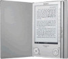
Sony PRS-505/SC Service Manual - Page 54
Prs-505, Diagrams - screen replacement
 |
View all Sony PRS-505/SC manuals
Add to My Manuals
Save this manual to your list of manuals |
Page 54 highlights
PRS-505 2. DIAGRAMS THIS NOTE IS COMMON FOR PRINTED WIRING BOARDS AND SCHEMATIC DIAGRAMS. (In addition to this, the necessary note is printed in each block.) For Printed Wiring Boards. Note: • Y : Parts extracted from the conductor side. • f : internal component. • : Pattern from the side which enables seeing. (The other layers' patterns are not indicated.) Caution: Parts face side: (Conductor side) Pattern face side: (Component side) Parts on the parts face side seen from the pattern face are indicated. Parts on the pattern face side seen from the parts face are indicated. • MAIN board is multi-layer printed board. However, the patterns of intermediate-layers have not been included in diagrams. * Replacing of IC1001 on the MAIN board used in this set requires a special tool. • Lead layouts surface Lead layout of conventional IC CSP (Chip Size Package) For Schematic Diagrams. Note: • All capacitors are in μF unless otherwise noted. (p: pF) 50 WV or less are not indicated except for electrolytics and tantalums. • All resistors are in Ω and 1/4 W or less unless otherwise specified. • f : internal component. • C : panel designation. Note: The components identified by mark 0 or dotted line with mark 0 are critical for safety. Replace only with part number specified. Note: Les composants identifiés par une marque 0 sont critiques pour la sécurité. Ne les remplacer que par une piéce portant le numéro spécifié. • A : B+ Line. • B : B- Line. • C : adjustment for repair. • Power voltage is dc 5.2V and fed with regulated dc power supply from TP402 and TP400 on the MAIN board. • Voltages are dc with respect to ground under no-signal (detuned) conditions. no mark : POWER ON ( ) : AUDIO PLAY * : Impossible to measure (For this model, the voltage is produced only when the screen is changed. Under the power on, there is a voltage that is not produced.) • Voltages are taken with VOM (Input impedance 10 MΩ). Voltage variations may be noted due to normal production tolerances. • Signal path. F : AUDIO L : VIDEO N : USB O : SD MEMORY CARD/MEMORY STICK DUO * Replacing of IC1001 on the MAIN board used in this set requires a special tool. • The voltage and waveform of CSP (chip size package) cannot be measured, because its lead is different feom that conventional IC. PRS-505 2 2
-
 1
1 -
2
-
3
-
4
-
5
-
6
-
7
-
8
-
9
-
10
-
11
-
12
-
13
-
14
-
15
-
16
-
17
-
18
-
19
-
20
-
21
-
22
-
23
-
24
-
25
-
26
-
27
-
28
-
29
-
30
-
31
-
32
-
33
-
34
-
35
-
36
-
37
-
38
-
39
-
40
-
41
-
42
-
43
-
44
-
45
-
46
-
47
-
48
-
 49
49 -
 50
50 -
 51
51 -
 52
52 -
 53
53 -
 54
54 -
 55
55 -
 56
56 -
 57
57 -
 58
58 -
 59
59 -
60
-
61
-
62
-
63
-
64
-
65
-
66
-
67
-
68
-
69
-
70
-
71
-
72
-
73
-
74
 |
 |
