Hitachi 43FDX01B Service Manual - Page 22
EN 22, LGE PDP 2K6
 |
View all Hitachi 43FDX01B manuals
Add to My Manuals
Save this manual to your list of manuals |
Page 22 highlights
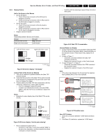
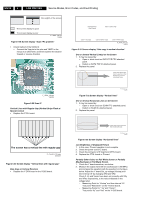
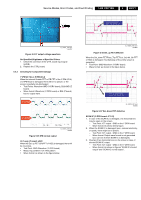
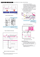
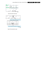
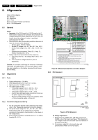
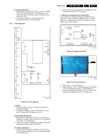
EN 22 5. LGE PDP 2K6 Service Modes, Error Codes, and Fault Finding - Test Point: Output TP of GND-TCP - Wave format: As shown in figure below. In case of normal wave output, when STB signal is generated, the output must maintain "HIGH". When STB signal is generated again, the output must fall to "LOW". But when the TCP IC is damaged, the STB signal is not generated, and the output falls to "LOW". 2. In case of IC damage, the screen may show no image on the corresponding part, or mis-discharge. In most cases you can see a burn mark on the IC. - Test Point: Output TP of GND-TCP - Wave format: No output wave. Figure 5-38 SCAN IC defective G_16390_052.eps 150806 115V ~‹Œ•G›ŒGw 7us 60V i™Œˆ’G›ŒGzjhuGwœ“šŒ k G•G G– zjhuGwœ“šŒ F_15590_031.eps 040705 Figure 5-39 SCAN IC shorted output p›'šG–œ›G–G–™‹Œ™G–œ›—œ› p•GŠˆšŒG–G•–™”ˆ“G SG›G”ˆ Gš–žG ˆšGˆG‹–››Œ‹G“•Œ F_15590_033.eps 060605 Figure 5-41 COF IC output defective G_16390_053.eps 150806 Figure 5-40 SCAN IC normal output wave TCPs 1. In case of shorting or opening of TCP IC output, the screen may show one or several vertical lines. F_15590_034.eps 060605 Figure 5-42 TCP normal output Crystal (CTRL board: X1) 1. When a crystal is damaged, the screen is not shown. - Test Point: 3-pin of GND-Crystal (CTRL board: X1). - Wave format: Output wave is not generated. 2. In case of unusual start-up of the crystal, the screen may blink. - Wave format: As shown in figure below. - Measurement position: Measuring output 3-pin of crystal (CTRL board: X1).
-
 1
1 -
2
-
3
-
4
-
5
-
6
-
7
-
8
-
9
-
10
-
11
-
12
-
13
-
14
-
15
-
16
-
 17
17 -
 18
18 -
 19
19 -
 20
20 -
 21
21 -
 22
22 -
 23
23 -
 24
24 -
 25
25 -
 26
26 -
 27
27 -
28
-
29
-
30
-
31
-
32
-
33
-
34
 |
 |
