Hitachi 43FDX01B Service Manual - Page 30
EN 30, LGE PDP 2K6
 |
View all Hitachi 43FDX01B manuals
Add to My Manuals
Save this manual to your list of manuals |
Page 30 highlights
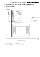
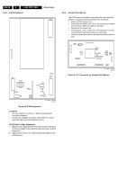
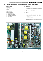
EN 30 9. LGE PDP 2K6 Circuit Descriptions, Abbreviation List, and IC Data Sheets 9.2.2 Power ON and Power OFF Sequence • For a correct functioning of the display, the different supply voltages have to be powered up and down according to a certain sequence. This sequence is shown in the following figure. Vcc (5V) Va Vs DISPEN TOn TVaR TVsR Power_on 3 Sec Min. 5 frames Normal Display TOff TVaF TVsF Power_off 3 Sec Min. 2 frame Symbol TOn TOff TVaR TVaF TVsR TVsF Description Time interval between 90% of Vcc and 10% of Vs when Power On Time interval between 10% of Vs and 90% of Vcc when Power Off Rising Time of Va (10% to 90%) Falling Time of Va (90% to 10%) Rising Time of Vs (10% to 90%) Falling Time of Vs (90% to 10%) Min. Max. unit 0.2 - sec 20 - ms 10 400 ms 100 300 ms 100 800 ms 90 500 ms ቁ If power sequence does not meet to above sequence diagram, PDP drivers may be damaged permanently. ቁ Even when AC input power supply is switched ON/OFF, above sequence should be observed strictly. ත Transition section: Transition section is needed to drive PDP as a initial and set-up period. At this period, Brightness is low and there is no gray. ත If DISPEN is low, picture is changed to BLACK pattern. Signal is operated by synchronized vertical signal. ත The panel will not malfunction, if DISPEN is high at start up. G_16390_080.eps 310806 Figure 9-2 Power supply sequence 9.3 Control Board 9.3.1 Purpose Creates signal processing, and controls many FETs on each DRIVER board with R, G, and B signals. 9.4 X Board 9.4.1 Purpose Receives LOGIC signal from the CONTROL board and makes the ADDRESS PULSE (generates Address discharge) by ON/ OFF operation, and then supplies this waveform to TCP (data). MCM (Multi Chip Module) LVDS Signal Input pin 8 bit or 10 MCM 6 bi t signal bit signal ( Multi Chip Module ) TCP G_16390_035.eps 100806 Figure 9-3 Control board X Left board X Right board Figure 9-4 X boards G_16390_083.eps 010906
-
 1
1 -
2
-
3
-
4
-
5
-
6
-
7
-
8
-
9
-
10
-
11
-
12
-
13
-
14
-
15
-
16
-
17
-
18
-
19
-
20
-
21
-
22
-
23
-
24
-
 25
25 -
 26
26 -
 27
27 -
 28
28 -
 29
29 -
 30
30 -
 31
31 -
 32
32 -
 33
33 -
 34
34
 |
 |
