Sony MHC-NX1 Service Manual - Page 12
Diagrams, Printed, Wiring, Boards, Schematic
 |
View all Sony MHC-NX1 manuals
Add to My Manuals
Save this manual to your list of manuals |
Page 12 highlights
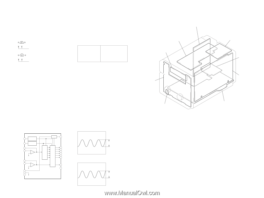
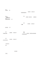
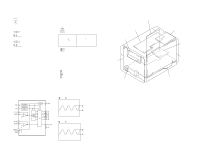
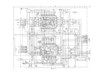
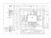
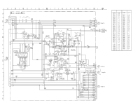
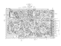
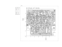
SECTION 5 DIAGRAMS 5-1. NOTE FOR PRINTED WIRING BOARDS AND SCHEMATIC DIAGRAMS Note on Printed Wiring Board: • X : parts extracted from the component side. • Y : parts extracted from the conductor side. • x : parts mounted on the conductor side. • b : Pattern from the side which enables seeing. (The other layers' patterns are not indicated) • Indication of transistor. Q BCE Q These are omitted. BCE These are omitted. Note on Schematic Diagram: • All capacitors are in µF unless otherwise noted. pF: µµF 50 WV or less are not indicated except for electrolytics and tantalums. • All resistors are in Ω and 1/4 W or less unless otherwise specified. • f : internal component. • 2 : nonflammable resistor. • 5 : fusible resistor. • C : panel designation. Note: The components identified by mark 0 or dotted line with mark 0 are critical for safety. Replace only with part number specified. Note: Les composants identifiés par une marque 0 sont critiques pour la sécurité. Ne les remplacer que par une pièce portant le numéro spécifié. • U : B+ Line. • V : B- Line. • Voltages and waveforms are dc with respect to ground under no-signal (detuned) conditions. no mark : TUNER (FM) • Voltages are taken with a VOM (Input impedance 10 MΩ). Voltage variations may be noted due to normal produc- tion tolerances. • Waveforms are taken with a oscilloscope. Voltage variations may be noted due to normal produc- tion tolerances. • Circled numbers refer to waveforms. • Signal path. F : TUNER (FM) E : TAPE PLAYBACK G : RECORD J : CD PLAY N : MIC INPUT • Abbreviation AUS : Australian model MY : Malaysia model CND : Canadian model SP : Singapore model JE : Tourist model TH : Thai model KR : Korean model • IC Block Diagram - MAIN Board - IC401 BA3830F R02 1 R01 2 LINE NF 3 LINE IN 4 REFERENCE CURRENT REFERENCE CURRENT - + REC NF 5 REC IN 6 - + RESET C 7 BIAS C 8 GND 9 RESET 18 RESET BAND PASS FILTER DET 17 F01 16 F02 15 F03 14 F04 13 F05 12 F06 11 REC LEVEL 10 VCC • Waveforms - MAIN Board - 1 IC501 q; (XCIN) 32.768 kHz 2 IC501 qd (XOUT) 1.4 Vp-p 3 Vp-p • Circuit Boards Location SUB TRANS board (US, Canadian, AEP, UK) TRANS board BACK LIGHT board PANEL baord R board 16 MHz 11 11 TUNER pack SURROUND AMP board (NX3) MAIN board PA board
-
 1
1 -
2
-
3
-
4
-
5
-
6
-
 7
7 -
 8
8 -
 9
9 -
 10
10 -
 11
11 -
 12
12 -
 13
13 -
 14
14 -
 15
15 -
 16
16 -
 17
17 -
18
-
19
-
20
-
21
-
22
-
23
-
24
-
25
-
26
-
27
-
28
-
29
-
30
-
31
-
32
-
33
-
34
-
35
-
36
-
37
-
38
-
39
-
40
-
41
-
42
-
43
-
44
-
45
-
46
-
47
-
48
-
49
-
50
-
51
-
52
-
53
-
54
-
55
-
56
-
57
-
58
-
59
-
60
-
61
-
62
-
63
-
64
-
65
-
66
-
67
-
68
-
69
-
70
-
71
-
72
-
73
-
74
-
75
-
76
-
77
-
78
-
79
-
80
-
81
-
82
-
83
-
84
-
85
-
86
-
87
-
88
-
89
-
90
-
91
-
92
-
93
-
94
-
95
-
96
-
97
 |
 |