Sony MHC-NX1 Service Manual - Page 45

SERVICING NOTES, NOTES, LASER, DIODE, EMISSION, CHECK, Notes on chip component replacement - repair

Page 45 highlights

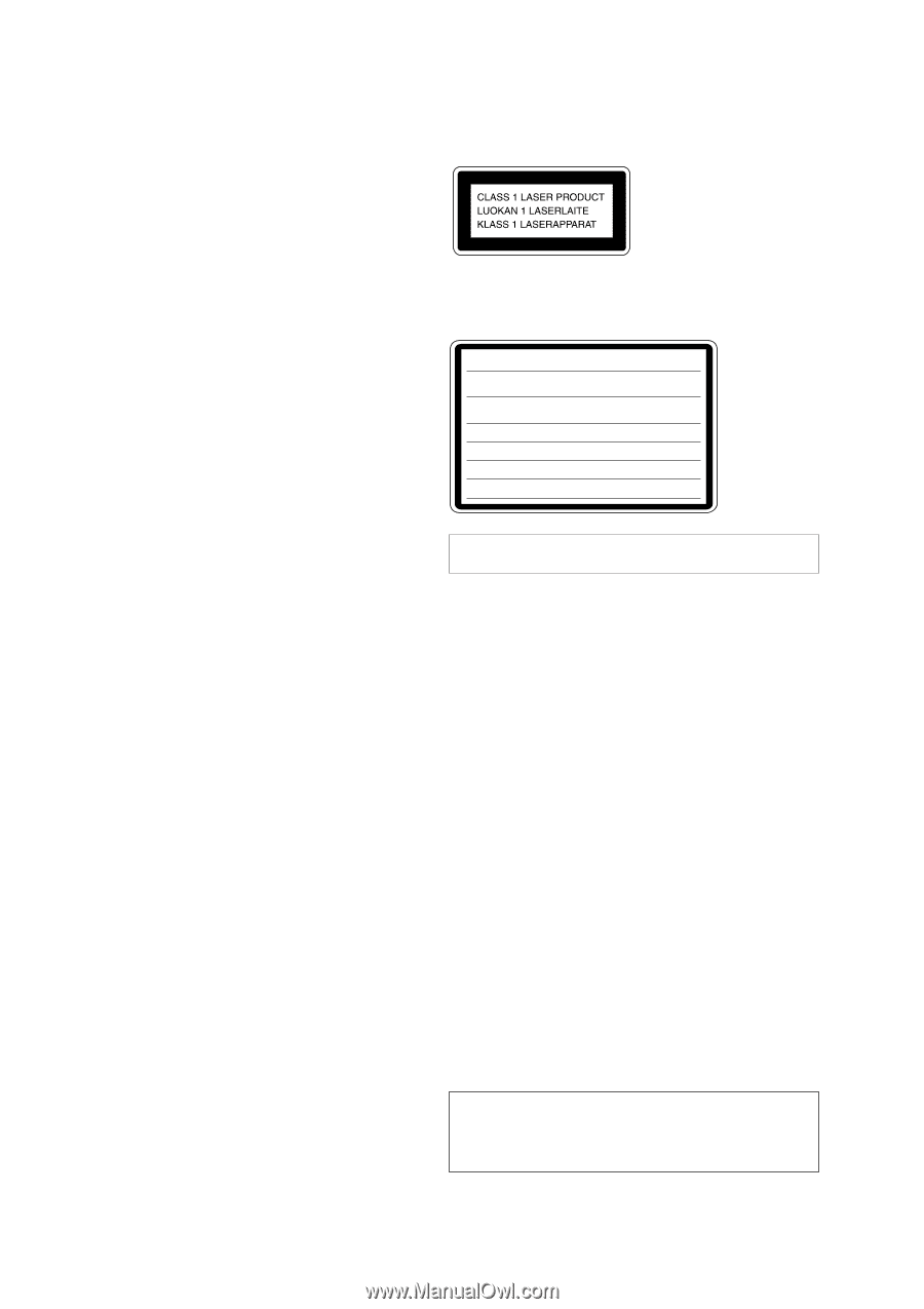
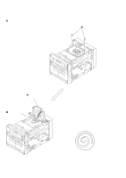
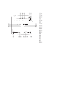
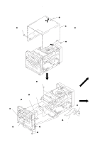
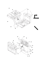
TABLE OF CONTENTS 1. SERVICING NOTES 2 2. GENERAL Location of Controls 5 3. DISASSEMBLY 6 4. TEST MODE 13 5. MECHANICAL ADJUSTMENTS 14 6. ELECTRICAL ADJUSTMENTS TAPE DECK Section 14 CD Section 17 7. DIAGRAMS 7-1. Note for Printed Wiring Boards and Schematic Diagrams 19 7-2. Printed Wiring Board - BD Board 20 7-3. Schematic Diagram - BD Board 21 7-4. Printed Wiring Boards - CD MOTOR/SENSOR Section 22 7-5. Schematic Diagram - CD MOTOR/SENSOR Section 23 7-6. Printed Wiring Board - AUDIO Board 24 7-7. Schematic Diagram - AUDIO Board 25 7-8. Printed Wiring Board - LEAF SW Board 26 7-9. Schematic Diagram - LEAF SW Board 26 7-10. Printed Wiring Board - MAIN Board 27 7-11. Schematic Diagram - MAIN Board (1/2 28 7-12. Schematic Diagram - MAIN Board (2/2 29 7-13. Printed Wiring Boards - PANEL Section 30 7-14. Schematic Diagram - PANEL Section 31 7-15. IC Pin Function Description 34 8. EXPLODED VIEWS 37 9. ELECTRICAL PARTS LIST 44 SAFETY-RELATED COMPONENT WARNING!! COMPONENTS IDENTIFIED BY MARK ! OR DOTTED LINE WITH MARK ! ON THE SCHEMATIC DIAGRAMS AND IN THE PARTS LIST ARE CRITICAL TO SAFE OPERATION. REPLACE THESE COMPONENTS WITH SONY PARTS WHOSE PART NUMBERS APPEAR AS SHOWN IN THIS MANUAL OR IN SUPPLEMENTS PUBLISHED BY SONY. ATTENTION AU COMPOSANT AYANT RAPPORT À LA SÉCURITÉ! LES COMPOSANTS IDENTIFIÉS PAR UNE MARQUE ! SUR LES DIAGRAMMES SCHÉMATIQUES ET LA LISTE DES PIÈCES SONT CRITIQUES POUR LA SÉCURITÉ DE FONCTIONNEMENT. NE REMPLACER CES COMPOSANTS QUE PAR DES PIÈCES SONY DONT LES NUMÉROS SONT DONNÉS DANS CE MANUEL OU DANS LES SUPPLÉMENTS PUBLIÉS PAR SONY. 2 SECTION 1 SERVICING NOTES This appliance is classified as a CLASS 1 LASER product. The CLASS 1 LASER PRODUCT MARKING is located on the rear exterior. Laser component in this product is capable of emitting radiation exceeding the limit for Class 1. The following caution label is located inside the unit. CAUTION : INVISIBLE LASER RADIATION WHEN OPEN AND INTERLOCKS DEFEATED. AVOID EXPOSURE TO BEAM. ADVARSEL : USYNLIG LASERSTRÅLING VED ÅBNING NÅR SIKKERHEDSAFBRYDERE ER UDE AF FUNKTION. UNDGÅ UDSAETTELSE FOR STRÅLING. VORSICHT : UNSICHTBARE LASERSTRAHLUNG, WENN ABDECKUNG GEÖFFNET UND SICHEREITSVERRIEGELUNG ÜBERBRÜCKT. NICHT DEM STRAHL AUSSETZEN. VARO! : AVATTAESSA JA SUOJALUKITUS OHITETTAESSA OLET ALT- TIINA NÄKYMÄTTÖMÄLLE LASERSÄTEILYLLE. ÄLÄ KATSO SÄTEESEEN. VARNING : OSYNLING LASERSTRÅLING NÄR DENNA DEL ÄR ÖPPNAD OCH SPÄRREN ÄR URKOPPLAD. BETRAKTA EJ STRÅLEN. ADVERSEL : USYNLIG LASERSTRÅLING NÅR DEKSEL ÅPNES OG SIKKERHEDSLÅS BRYTES. UNNGÅ EKSPONERING FOR STRÅLEN. VIGYAZAT! : A BURKOLAT NYITÁSAKOR LÁTHATATLAN LÉZERSU- GÁRVESZÉLY! KERÜLJE A BESUGÁRZÁST! NOTES ON HANDLING THE OPTICAL PICK-UP BLOCK OR BASE UNIT The laser diode in the optical pick-up block may suffer electrostatic break-down because of the potential difference generated by the charged electrostatic load, etc. on clothing and the human body. During repair, pay attention to electrostatic break-down and also use the procedure in the printed matter which is included in the repair parts. The flexible board is easily damaged and should be handled with care. NOTES ON LASER DIODE EMISSION CHECK The laser beam on this model is concentrated so as to be focused on the disc reflective surface by the objective lens in the optical pick-up block. Therefore, when checking the laser diode emission, observe from more than 30 cm away from the objective lens. Notes on chip component replacement • Never reuse a disconnected chip component. • Notice that the minus side of a tantalum capacitor may be dam- aged by heat. Flexible Circuit Board Repairing • Keep the temperature of the soldering iron around 270 ˚C dur- ing repairing. • Do not touch the soldering iron on the same conductor of the circuit board (within 3 times). • Be careful not to apply force on the conductor when soldering or unsoldering. CAUTION Use of controls or adjustments or performance of procedures other than those specified herein may result in hazardous radiation exposure.

  • 1
  • 2
  • 3
  • 4
  • 5
  • 6
  • 7
  • 8
  • 9
  • 10
  • 11
  • 12
  • 13
  • 14
  • 15
  • 16
  • 17
  • 18
  • 19
  • 20
  • 21
  • 22
  • 23
  • 24
  • 25
  • 26
  • 27
  • 28
  • 29
  • 30
  • 31
  • 32
  • 33
  • 34
  • 35
  • 36
  • 37
  • 38
  • 39
  • 40
  • 41
  • 42
  • 43
  • 44
  • 45
  • 46
  • 47
  • 48
  • 49
  • 50
  • 51
  • 52
  • 53
  • 54
  • 55
  • 56
  • 57
  • 58
  • 59
  • 60
  • 61
  • 62
  • 63
  • 64
  • 65
  • 66
  • 67
  • 68
  • 69
  • 70
  • 71
  • 72
  • 73
  • 74
  • 75
  • 76
  • 77
  • 78
  • 79
  • 80
  • 81
  • 82
  • 83
  • 84
  • 85
  • 86
  • 87
  • 88
  • 89
  • 90
  • 91
  • 92
  • 93
  • 94
  • 95
  • 96
  • 97

2
ATTENTION
AU
COMPOSANT
AYANT
RAPPORT
À
LA
SÉCURITÉ!
LES
COMPOSANTS
IDENTIFIÉS
PAR
UNE
MARQUE
!
SUR
LES
DIAGRAMMES
SCHÉMATIQUES
ET
LA
LISTE
DES
PIÈCES
SONT
CRITIQUES
POUR
LA
SÉCURITÉ
DE
FONCTIONNEMENT.
NE
REMPLACER
CES
COM-
POSANTS
QUE
PAR
DES
PIÈCES
SONY
DONT
LES
NUMÉROS
SONT
DONNÉS
DANS
CE
MANUEL
OU
DANS
LES
SUPPLÉMENTS
PUBLIÉS
PAR
SONY.
SAFETY-RELATED
COMPONENT
WARNING!!
COMPONENTS
IDENTIFIED
BY
MARK
!
OR
DOTTED
LINE
WITH
MARK
!
ON
THE
SCHEMATIC
DIAGRAMS
AND
IN
THE
PARTS
LIST
ARE
CRITICAL
TO
SAFE
OPERATION.
REPLACE
THESE
COMPONENTS
WITH
SONY
PARTS
WHOSE
PART
NUMBERS
APPEAR
AS
SHOWN
IN
THIS
MANUAL
OR
IN
SUPPLEMENTS
PUB-
LISHED
BY
SONY.
TABLE
OF
CONTENTS
1.
SERVICING
NOTES
...............................................
2
2.
GENERAL
Location of Controls
.......................................................
5
3.
DISASSEMBLY
.........................................................
6
4.
TEST
MODE
..............................................................
13
5.
MECHANICAL
ADJUSTMENTS
.......................
14
6.
ELECTRICAL
ADJUSTMENTS
TAPE DECK Section
......................................................
14
CD Section
......................................................................
17
7.
DIAGRAMS
7-1.
Note for Printed Wiring Boards and
Schematic Diagrams
.......................................................
19
7-2.
Printed Wiring Board
– BD Board –
.............................
20
7-3.
Schematic Diagram
– BD Board –
................................
21
7-4.
Printed Wiring Boards
– CD MOTOR/SENSOR Section –
................................
22
7-5.
Schematic Diagram
– CD MOTOR/SENSOR Section –
................................
23
7-6.
Printed Wiring Board
– AUDIO Board –
......................
24
7-7.
Schematic Diagram
– AUDIO Board –
.........................
25
7-8.
Printed Wiring Board
– LEAF SW Board –
..................
26
7-9.
Schematic Diagram
– LEAF SW Board –
.....................
26
7-10.
Printed Wiring Board
– MAIN Board –
........................
27
7-11.
Schematic Diagram
– MAIN Board (1/2) –
..................
28
7-12.
Schematic Diagram
– MAIN Board (2/2) –
..................
29
7-13.
Printed Wiring Boards
– PANEL Section –
..................
30
7-14.
Schematic Diagram
– PANEL Section –
.......................
31
7-15.
IC Pin Function Description
...........................................
34
8.
EXPLODED
VIEWS
................................................
37
9.
ELECTRICAL
PARTS
LIST
...............................
44
SECTION
1
SERVICING
NOTES
The laser diode in the optical pick-up block may suffer electro-
static break-down because of the potential difference generated
by the charged electrostatic load, etc. on clothing and the human
body.
During repair, pay attention to electrostatic break-down and also
use the procedure in the printed matter which is included in the
repair parts.
The flexible board is easily damaged and should be handled with
care.
NOTES
ON
LASER
DIODE
EMISSION
CHECK
The laser beam on this model is concentrated so as to be focused
on the disc reflective surface by the objective lens in the optical
pick-up block. Therefore, when checking the laser diode emis-
sion, observe from more than 30 cm away from the objective lens.
Notes on chip component replacement
Never reuse a disconnected chip component.
Notice that the minus side of a tantalum capacitor may be dam-
aged by heat.
Flexible Circuit Board Repairing
Keep the temperature of the soldering iron around 270 ˚C dur-
ing repairing.
Do not touch the soldering iron on the same conductor of the
circuit board (within 3 times).
Be careful not to apply force on the conductor when soldering
or unsoldering.
NOTES
ON
HANDLING
THE
OPTICAL
PICK-UP
BLOCK
OR
BASE
UNIT
CAUTION
Use of controls or adjustments or performance of procedures
other than those specified herein may result in hazardous ra-
diation exposure.
This appliance is classified as a CLASS 1 LASER product.
The CLASS 1 LASER PRODUCT MARKING is located on
the rear exterior.
Laser component in this product is capable of emitting radiation
exceeding the limit for Class 1.
The following caution label is located inside the unit.
CAUTION
:
INVISIBLE
LASER
RADIATION
WHEN
OPEN
AND
INTERLOCKS
DEFEATED.
AVOID
EXPOSURE
TO
BEAM.
ADVARSEL :
USYNLIG
LASERSTRÅLING
VED
ÅBNING
NÅR
SIKKERHEDSAFBRYDERE
ER
UDE
AF
FUNKTION.
UNDGÅ
UDSAETTELSE
FOR
STRÅLING.
VORSICHT
:
UNSICHTBARE
LASERSTRAHLUNG,
WENN
ABDECKUNG
GEÖFFNET
UND
SICHEREITSVERRIEGELUNG
ÜBERBRÜCKT.
NICHT
DEM
STRAHL
AUSSETZEN.
VARO
!
:
AVATTAESSA JA SUOJALUKITUS OHITETTAESSA OLET ALT-
TIINA
NÄKYMÄTTÖMÄLLE
LASERSÄTEILYLLE.
ÄLÄ
KATSO
SÄTEESEEN.
VARNING
:
OSYNLING LASERSTRÅLING NÄR DENNA
DEL ÄR ÖPPNAD
OCH SPÄRREN ÄR URKOPPLAD. BETRAKTA EJ STRÅLEN.
ADVERSEL :
USYNLIG
LASERSTRÅLING
NÅR
DEKSEL
ÅPNES
OG
SIKKERHEDSLÅS BRYTES.
UNNGÅ EKSPONERING FOR STRÅLEN.
VIGYAZAT
!
:
A
BURKOLAT
NYITÁSAKOR
LÁTHATATLAN
LÉZERSU-
GÁRVESZÉLY
!
KERÜLJE
A
BESUGÁRZÁST
!