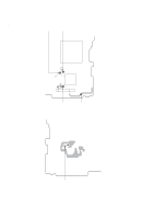
Sony MZ-R50 Service Manual - Page 37
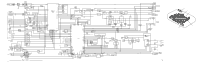
Pin No., Pin name, Description, IC801, SYSTEM CONTROL CXP81960M-652R - remote
 |
View all Sony MZ-R50 manuals
Add to My Manuals
Save this manual to your list of manuals |
Page 37 highlights
IC801 SYSTEM CONTROL (CXP81960M-652R) Pin No. 1 2 3 4 5 6 7 8 9 10 11 12 13 14 15 16 17 18 19 20 21 22 23 24 25 26 27 28 29 30 31 32 33 34 35 36 37 38 39 40 41 42 43 44 45 46 47 48 49 50 Pin name CLCS XRST WRPWR TX SENSE LDON XSHOCK ---- INLS PROTECT DATA HOLD WP OPEN CLOCK CLK SDIO EVR DATA PUSH JOG LCD STB CL SCK SDI2 SYNC REC D. B. B XLINEDET AVLS XTEST XDCIN KANA SE L AM3 ON XP CONT LIP ON XREC LED MODE2 MODE1 XRF STBY XLCD ON MP XMRST VSS XTAL EXTAL CS ---- LCD DATA LCD SCK ---- ---- HIDCMNT KEYR AVSS I/O Description O Chip select output to real time clock (IC804). O Reset output. L : Reset O Laser power switching signal output. O Write data transfer timing output. I Internal status (SENSE) input. O Laser ON signal. H : ON I Track jump detection input. - Not used (Open). I Detecting switch for internal circuit of sleding. Internal circuit : L I Disc write protect switch. H : Protect O Data output to remote control. I Hold switch input (This unit). L : Hold I Wake-up signal input from remote control key and this unit key. I Detecting switch for opening and closing of the upper cover. Close : L I CLOCK SET switch input. I Serial clock input. I Electric volume control data input. I Push JOG switch input. O LCD standby output. O Serial clock output for real time clock (IC804). I Serial data input. I SYNCHRO REC switch input. I DIGITAL MEGA BASS switch input. I Line input detect. L : Line I AVLS switch input. L : ON I Test mode terminal. L : Test mode I DC input detect. L : DC IN - Not used (Fixed at "H"). O This is at "H" level during external battery operation. O Power control output. L : ON O Outputs H while operating with a lithium battery. O REC LED control. L : ON O Head drive (IC506) control signal output. O O Power control output to RF amplifier (IC501). O LCD ON/OFF control. L : ON - Microprocessor mode input (Fixed at "L"). I Microprocessor reset input. - Ground. - System clock (12MHz). - System clock (12MHz). - Chip Select input (Connected to +2.8V). - Not used (Fixed at "L"). O LCD data output. O Serial clock output. - Not used (Open). - Not used (Open). I Voltage monitor DC input. I Remote control key input. - Ground terminal for A/D converter. - 37 -
-
 1
1 -
2
-
3
-
4
-
5
-
6
-
7
-
8
-
9
-
10
-
11
-
12
-
13
-
14
-
15
-
16
-
17
-
18
-
19
-
20
-
21
-
22
-
23
-
24
-
25
-
26
-
27
-
28
-
29
-
30
-
31
-
 32
32 -
 33
33 -
 34
34 -
 35
35 -
 36
36 -
 37
37 -
 38
38 -
 39
39 -
 40
40 -
 41
41 -
 42
42 -
43
-
44
-
45
-
46
-
47
-
48
-
49
-
50
-
51
-
52
-
53
-
54
-
55
-
56
 |
 |