Sony MZ-R50 Service Manual - Page 41
Schematic Diagram - Main 2/3
 |
View all Sony MZ-R50 manuals
Add to My Manuals
Save this manual to your list of manuals |
Page 41 highlights
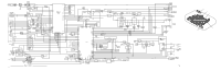
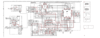
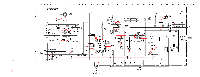
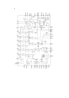
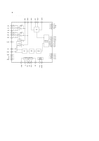
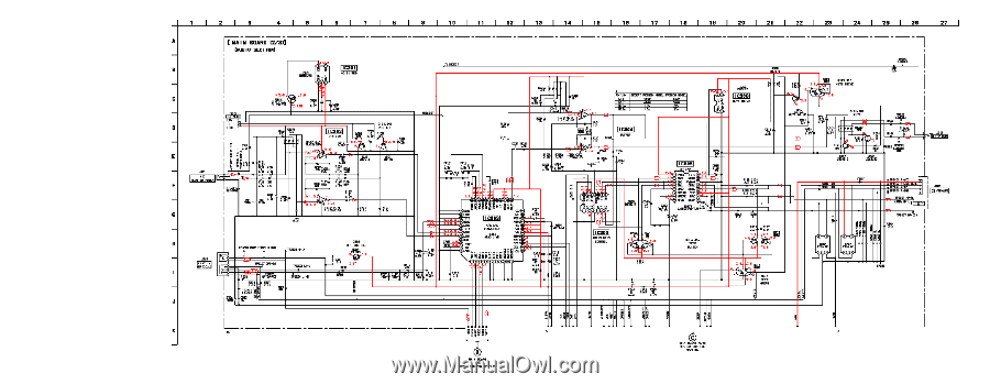
MZ-R50 6-6. SCHEMATIC DIAGRAM - MAIN (2/3) SECTION - r Refer to page 62 for IC Block Diagrams. Note: • All capacitors are in µF unless otherwise noted. pF: µµF 50 WV or less are not indicated except for electrolytics and tantalums. • All resistors are in Ω and 1/4 W or less unless otherwise specified. • A : B+ Line. • Power voltage is dc 6V and fed with regulated dc power supply from external power voltage jack (J901). • Voltages and waveforms are dc with respect to ground under no-signal conditions. no mark : PB ( ) : REC • Voltages are taken with a VOM (Input impedance 10 MΩ). Voltage variations may be noted due to normal produc- tion tolerances. • Signal path. E : PB a : REC N : MIC - 53 - - 54 - - 55 - - 56 -
-
 1
1 -
2
-
3
-
4
-
5
-
6
-
7
-
8
-
9
-
10
-
11
-
12
-
13
-
14
-
15
-
16
-
17
-
18
-
19
-
20
-
21
-
22
-
23
-
24
-
25
-
26
-
27
-
28
-
29
-
30
-
31
-
32
-
33
-
34
-
35
-
 36
36 -
 37
37 -
 38
38 -
 39
39 -
 40
40 -
 41
41 -
 42
42 -
 43
43 -
 44
44 -
 45
45 -
 46
46 -
47
-
48
-
49
-
50
-
51
-
52
-
53
-
54
-
55
-
56
 |
 |
– 55 –
– 56 –
– 53 –
– 54 –
MZ-R50
r
Refer to page 62 for IC Block Diagrams.
6-6. SCHEMATIC DIAGRAM – MAIN (2/3) SECTION –
Note:
•
All capacitors are in
μ
F unless otherwise noted.
pF:
μμ
F
50 WV or less are not indicated except for electrolytics
and tantalums.
•
All resistors are in
Ω
and
1
/
4
W or less unless otherwise
specified.
•
A
: B+ Line.
•
Power voltage is dc 6V and fed with regulated dc power
supply from external power voltage jack (J901).
•
Voltages and waveforms are dc with respect to ground
under no-signal conditions.
no mark
: PB
(
)
: REC
•
Voltages are taken with a VOM (Input impedance 10 M
Ω
).
Voltage variations may be noted due to normal produc-
tion tolerances.
•
Signal path.
E
: PB
a
: REC
N
: MIC