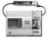
Sony MZ-R50 Service Manual - Page 38
Sony MZ-R50 - MD Walkman MiniDisc Recorder Manual
 |
View all Sony MZ-R50 manuals
Add to My Manuals
Save this manual to your list of manuals |
Page 38 highlights
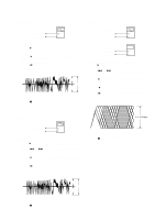
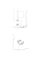
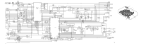
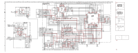
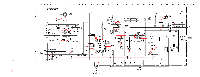
Pin No. 51 52 53 54 55 56 57 58 59 60 61 62 63 64 65 66 67 68 69 70 71 72 73 74 75 76 77 78 79 80 81 82 83 84 85 86 87 88 89 90 91 92 93 94 95 96 97 98 99 100 Pin name AVREF AVDD AM3 MNT TEMP KEY3 KEY4 KEY0 KEY1 UNREG MNT LIP MNT FG IN SLA SLB INT SW PACK IN JACKDET OPT DET MIC DET XLAT KEY ON ST1 A ST2 A ---- ---- DQSY T COUNT SDI1 SDO1 SCK1 SQSY BEEP XLIP DET REFLCT TEX XT VSS VDD NC XCS ADA XPD ADA ST1B ST2B A MUTE OPT CONT CS EVR CS NV SCK2 ------- SDO2 XLIP I/O Description I A/D converter reference voltage input. - A/D converter power supply terminal. I AC adaptor or EXT battery detection input. L : EXT battery I Temp meter (IC803) input. I PLAY/REC key input. I Key input. I Key input. I Key input. I UNREG voltage monitor. I Voltage monitor for lithium battery. I FG input from motor driver (IC701). I I JOG dial signal input. I INITIAL switch input. I MEDIA switch input. I Input jack detection input. I Detecting input an optical input. I MIC jack detection. O Latch output. O TRACK MARK jack input. O O Stepping motor control signal output. - Not used (Open). - Not used (Open). I Subcode Q sync (SCOR) of digital in U-bit CD format from IC503. I Traverse count signal input. I Serial data input. O Serial data output. O Serial clock output. I SUB-Q/ADIP SYNC input. O BEEP sound output control. H : BEEP sound output I This is at "L" level when using the lithium battery or with no sensor switch input. I CD/MO discrimination switch. - Not used (Fixed at "L") - Not used (Open). - Ground. - Power supply pin (+2.8V). - Not used (Fixed at "H") I Chip select input. O D/A converter power down detect during recording. H : Power down O O Stepping motor control signal output. O Analog mute control. L : Mute O Power supply control output for an optical input. O O Chip select output. O Serial clock output. O HF module control output. (Not used : open) O Serial data output. O Charge control. H : Charge - 38 -
-
 1
1 -
2
-
3
-
4
-
5
-
6
-
7
-
8
-
9
-
10
-
11
-
12
-
13
-
14
-
15
-
16
-
17
-
18
-
19
-
20
-
21
-
22
-
23
-
24
-
25
-
26
-
27
-
28
-
29
-
30
-
31
-
32
-
 33
33 -
 34
34 -
 35
35 -
 36
36 -
 37
37 -
 38
38 -
 39
39 -
 40
40 -
 41
41 -
 42
42 -
 43
43 -
44
-
45
-
46
-
47
-
48
-
49
-
50
-
51
-
52
-
53
-
54
-
55
-
56
 |
 |