AMD AX2000DMT3C User Guide - Page 48
General AC and DC Characteristics
 |
View all AMD AX2000DMT3C manuals
Add to My Manuals
Save this manual to your list of manuals |
Page 48 highlights
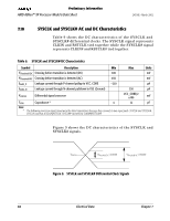
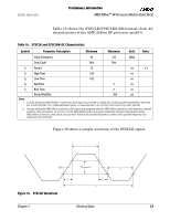
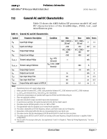
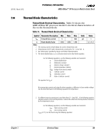
Preliminary Information AMD Athlon™ XP Processor Model 6 Data Sheet 24309E-March 2002 7.12 General AC and DC Characteristics Table 13 shows the AMD Athlon XP processor model 6 AC and DC characteristics of the Southbridge, JTAG, test, and miscellaneous pins. Table 13. General AC and DC Characteristics Symbol Parameter Description Condition Min Max Units Notes VIH Input High Voltage (VCC_CORE/2) + VCC_CORE + 200 mV 300 mV V 1, 2 VIL Input Low Voltage -300 350 mV 1, 2 VOH Output High Voltage VCC_CORE - 400 VCC_CORE + 300 mV VOL Output Low Voltage -300 400 mV ILEAK_P Tristate Leakage Pullup VIN = VSS -1 (Ground) mA ILEAK_N Tristate Leakage Pulldown VIN = VCC_CORE Nominal 600 µA IOH Output High Current -16 mA 3 IOL Output Low Current 16 mA 3 TSU Sync Input Setup Time 2.0 ns 4, 5 THD Sync Input Hold Time 0.0 ps 4, 5 TDELAY Output Delay with respect to RSTCLK 0.0 6.1 ns 5 Notes: 1. Characterized across DC supply voltage range. 2. Values specified at nominal VCC_CORE. Scale parameters between VCC_CORE minimum and VCC_CORE maximum. 3. IOL and IOH are measured at VOL max and VOH min, respectively. 4. Synchronous inputs/outputs are specified with respect to RSTCLK and RSTCK# at the pins. 5. These are aggregate numbers. 6. Edge rates indicate the range over which inputs were characterized. 7. In asynchronous operation, the signal must persist for this time to enable capture. 8. This value assumes RSTCLK period is 10 ns ==> TBIT = 2*fRST. 9. The approximate value for standard case in normal mode operation. 10. This value is dependent on RSTCLK frequency, divisors, Low Power mode, and core frequency. 11. Reassertions of the signal within this time are not guaranteed to be seen by the core. 12. This value assumes that the skew between RSTCLK and K7CLKOUT is much less than one phase. 13. This value assumes RSTCLK and K7CLKOUT are running at the same frequency, though the processor is capable of other configurations. 14. Time to valid is for any open drain pins. See requirements 7 and 8 in Chapter 8, "Power-Up Timing Requirements," for more information. 36 Electrical Data Chapter 7
-
 1
1 -
2
-
3
-
4
-
5
-
6
-
7
-
8
-
9
-
10
-
11
-
12
-
13
-
14
-
15
-
16
-
17
-
18
-
19
-
20
-
21
-
22
-
23
-
24
-
25
-
26
-
27
-
28
-
29
-
30
-
31
-
32
-
33
-
34
-
35
-
36
-
37
-
38
-
39
-
40
-
41
-
42
-
 43
43 -
 44
44 -
 45
45 -
 46
46 -
 47
47 -
 48
48 -
 49
49 -
 50
50 -
 51
51 -
 52
52 -
 53
53 -
54
-
55
-
56
-
57
-
58
-
59
-
60
-
61
-
62
-
63
-
64
-
65
-
66
-
67
-
68
-
69
-
70
-
71
-
72
-
73
-
74
-
75
-
76
-
77
-
78
-
79
-
80
-
81
-
82
-
83
-
84
-
85
-
86
-
87
-
88
-
89
-
90
-
91
-
92
-
93
-
94
 |
 |
