AMD AX2000DMT3C User Guide - Page 55
Signal and Power-Up Requirements, 8.1 Power-Up Requirements, Signal Sequence and Timing Description
 |
View all AMD AX2000DMT3C manuals
Add to My Manuals
Save this manual to your list of manuals |
Page 55 highlights
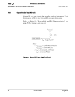
24309E-March 2002 Preliminary Information AMD Athlon™ XP Processor Model 6 Data Sheet 8 Signal and Power-Up Requirements The AMD Athlon™ XP processor model 6 is designed to provide functional operation if the voltage and temperature parameters are within the limits of normal operating ranges. 8.1 Power-Up Requirements Signal Sequence and Timing Description Figure 12 shows the relationship between key signals in the system during a power-up sequence. This figure details the requirements of the processor. 3.3 V Supply VCCA (2.5 V) (for PLL) VCC_CORE (Processor Core) RESET# NB_RESET# PWROK FID[3:0] System Clock 2 1 6 4 5 7 3 Warm reset condition 8 Figure 12. Signal Relationship Requirements During Power-Up Sequence Note: 1. Figure 12 represents several signals generically by using names not necessarily consistent with any pin lists or schematics. 2. Requirements 1-8 in Figure 12 are described in "Power-Up Timing Requirements" on page 44. Chapter 8 Signal and Power-Up Requirements 43
-
 1
1 -
2
-
3
-
4
-
5
-
6
-
7
-
8
-
9
-
10
-
11
-
12
-
13
-
14
-
15
-
16
-
17
-
18
-
19
-
20
-
21
-
22
-
23
-
24
-
25
-
26
-
27
-
28
-
29
-
30
-
31
-
32
-
33
-
34
-
35
-
36
-
37
-
38
-
39
-
40
-
41
-
42
-
43
-
44
-
45
-
46
-
47
-
48
-
49
-
 50
50 -
 51
51 -
 52
52 -
 53
53 -
 54
54 -
 55
55 -
 56
56 -
 57
57 -
 58
58 -
 59
59 -
 60
60 -
61
-
62
-
63
-
64
-
65
-
66
-
67
-
68
-
69
-
70
-
71
-
72
-
73
-
74
-
75
-
76
-
77
-
78
-
79
-
80
-
81
-
82
-
83
-
84
-
85
-
86
-
87
-
88
-
89
-
90
-
91
-
92
-
93
-
94
 |
 |
