Compaq 8000 Technical Reference Guide: HP Compaq 8000 Elite Series Business De - Page 38
Option ROM Mapping, 2.4 PCI Interrupts, 2.5 PCI Power Management Support, Link Layer
 |
UPC - 884420665106
View all Compaq 8000 manuals
Add to My Manuals
Save this manual to your list of manuals |
Page 38 highlights
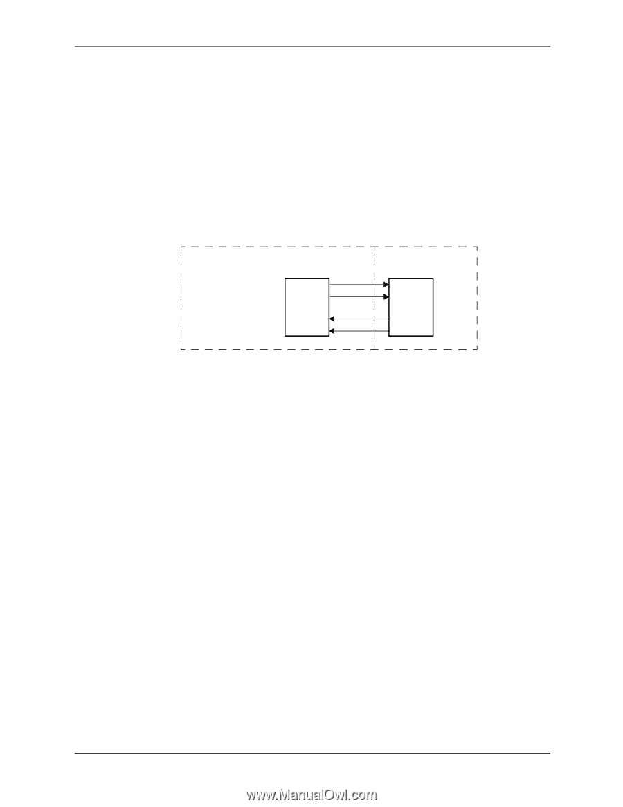
System Support Link Layer The link layer provides data integrity by adding a sequence information prefix and a CRC suffix to the packet created by the transaction layer. Flow-control methods ensure that a packet will only be transferred if the receiving device is ready to accomodate it. A corrupted packet will be automatically re-sent. Physical Layer The PCIe bus uses a point-to-point, high-speed TX/RX serial lane topology. One or more full-duplex lanes transfer data serially, and the design allows for scalability depending on end-point capabilities. Each lane consists of two differential pairs of signal paths; one for transmit, one for receive (Figure 4-1). System Board TX Device A RX PCI Express Card Device B Figure 4-1. PCIe Bus Lane Each byte is transferred using 8b/10b encoding. which embeds the clock signal with the data. Operating at a 2.5 Gigabit transfer rate, a single lane can provide a data flow of 200 MBps. The bandwidth is increased if additional lanes are available for use. During the initialization process, two PCIe devices will negotiate for the number of lanes available and the speed the link can operate at. In a x1 (single lane) interface, all data bytes are transferred serially over the lane. In a multi-lane interface, data bytes are distributed across the lanes using a multiplex scheme. 4.2.3 Option ROM Mapping During POST, the PCI bus is scanned for devices that contain their own specific firmware in ROM. Such option ROM data, if detected, is loaded into system memory's DOS compatibility area (refer to the system memory map shown in chapter 3). 4.2.4 PCI Interrupts Eight interrupt signals (INTA- thru INTH-) are available for use by PCI devices. These signals may be generated by on-board PCI devices or by devices installed in the PCI slots. For more information on interrupts including PCI interrupt mapping refer to the "System Resources" section 4.3. 4.2.5 PCI Power Management Support This system complies with the PCI Power Management Interface Specification (rev 1.0). The PCI Power Management Enable (PME-) signal is supported by the chipset and allows compliant PCI peripherals to initiate the power management routine. 4-4 www.hp.com Technical Reference Guide
-
 1
1 -
2
-
3
-
4
-
5
-
6
-
7
-
8
-
9
-
10
-
11
-
12
-
13
-
14
-
15
-
16
-
17
-
18
-
19
-
20
-
21
-
22
-
23
-
24
-
25
-
26
-
27
-
28
-
29
-
30
-
31
-
32
-
 33
33 -
 34
34 -
 35
35 -
 36
36 -
 37
37 -
 38
38 -
 39
39 -
 40
40 -
 41
41 -
 42
42 -
 43
43 -
44
-
45
-
46
-
47
-
48
-
49
-
50
-
51
-
52
-
53
-
54
-
55
-
56
-
57
-
58
-
59
-
60
-
61
-
62
-
63
-
64
-
65
-
66
-
67
-
68
-
69
-
70
-
71
-
72
-
73
-
74
-
75
-
76
-
77
-
78
-
79
-
80
-
81
-
82
-
83
-
84
-
85
-
86
-
87
-
88
-
89
-
90
-
91
-
92
-
93
-
94
-
95
-
96
-
97
-
98
-
99
-
100
-
101
-
102
-
103
-
104
-
105
-
106
-
107
-
108
-
109
-
110
-
111
-
112
-
113
-
114
 |
 |