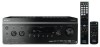
Sony STR DA2400ES Service Manual - Page 100
Sony STR DA2400ES - 7.1 Channel Home Theater AV Receiver Manual
 |
UPC - 027242729872
View all Sony STR DA2400ES manuals
Add to My Manuals
Save this manual to your list of manuals |
Page 100 highlights
STR-DA2400ES/DG920 Pin No. Pin Name I/O Description EM_D[6], EM_D[4], EM_D[2], EM_D[1], R5 to R13 EM_D[15], EM_D[13], I/O Two-way data bus with the SD-RAM EM_D[12], EM_D[10], EM_D[8] R14 EM_CLK O Clock signal output to the SD-RAM R15 EM_DQM[3] O Byte enable signal output to the SD-RAM R16 DVDD - Power supply terminal (+3.3V) (for IO) T1 VSS - Ground terminal T2 DVDD - Power supply terminal (+3.3V) (for IO) T3 EM_WE# O Write enable signal output to the SD-RAM T4 to T6 EM_D[7], EM_D[5], EM_D[3] I/O Two-way data bus with the SD-RAM T7 VSS - Ground terminal T8, T9 EM_D[0], EM_D[14] I/O Two-way data bus with the SD-RAM T10 VSS - Ground terminal T11, T12 EM_D[11], EM_D[9] I/O Two-way data bus with the SD-RAM T13 EM_DQM[1] O Byte enable signal output to the SD-RAM T14 EM_CKE O Clock enable signal output to the SD-RAM T15 DVDD - Power supply terminal (+3.3V) (for IO) T16 VSS - Ground terminal 100
-
 1
1 -
2
-
3
-
4
-
5
-
6
-
7
-
8
-
9
-
10
-
11
-
12
-
13
-
14
-
15
-
16
-
17
-
18
-
19
-
20
-
21
-
22
-
23
-
24
-
25
-
26
-
27
-
28
-
29
-
30
-
31
-
32
-
33
-
34
-
35
-
36
-
37
-
38
-
39
-
40
-
41
-
42
-
43
-
44
-
45
-
46
-
47
-
48
-
49
-
50
-
51
-
52
-
53
-
54
-
55
-
56
-
57
-
58
-
59
-
60
-
61
-
62
-
63
-
64
-
65
-
66
-
67
-
68
-
69
-
70
-
71
-
72
-
73
-
74
-
75
-
76
-
77
-
78
-
79
-
80
-
81
-
82
-
83
-
84
-
85
-
86
-
87
-
88
-
89
-
90
-
91
-
92
-
93
-
94
-
 95
95 -
 96
96 -
 97
97 -
 98
98 -
 99
99 -
 100
100 -
 101
101 -
 102
102 -
 103
103 -
 104
104 -
 105
105 -
106
-
107
-
108
-
109
-
110
-
111
-
112
-
113
-
114
-
115
-
116
-
117
-
118
-
119
-
120
-
121
-
122
-
123
-
124
-
125
-
126
-
127
-
128
-
129
-
130
-
131
-
132
-
133
-
134
-
135
-
136
-
137
-
138
-
139
-
140
-
141
-
142
-
143
-
144
 |
 |
