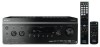
Sony STR DA2400ES Service Manual - Page 35
For Schematic Diagrams., For Printed Wiring Boards.
 |
UPC - 027242729872
View all Sony STR DA2400ES manuals
Add to My Manuals
Save this manual to your list of manuals |
Page 35 highlights
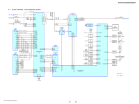
THIS NOTE IS COMMON FOR PRINTED WIRING BOARDS AND SCHEMATIC DIAGRAMS. (In addition to this, the necessary note is printed in each block.) For Printed Wiring Boards. Note: • X: Parts extracted from the component side. • Y: parts extracted from the conductor side. • f : internal component. • : Pattern from the side which enables seeing. (The other layers' patterns are not indicated.) Caution: Pattern face side: Parts on the pattern face side seen from (Conductor Side) the pattern face are indicated. Parts face side: Parts on the parts face side seen from (Component Side) the parts face are indicated. Caution: Pattern face side: (SIDE B) Parts face side: (SIDE A) Parts on the pattern face side seen from the pattern face are indicated. Parts on the parts face side seen from the parts face are indicated. • DIGITAL VIDEO and DSP boards are multi-layer printed boards. However, the patterns of intermediate-layers have not been included in diagrams. • Indication of transistor. C Q These are omitted. BE BC E These are omitted. ∗ Replacement of IC3601 on the DIGITAL VIDEO board used in this set requires a special tool. • Lead layouts surface For Schematic Diagrams. Note: • All capacitors are in μF unless otherwise noted. (p: pF) 50 WV or less are not indicated except for electrolytics and tantalums. • All resistors are in Ω and 1/4 W or less unless otherwise specified. • f : internal component. • 2: nonflammable resistor. • C : panel designation. Note: The components identified by mark 0 or dotted line with mark 0 are critical for safety. Replace only with part number specified. Note: Les composants identifiés par une marque 0 sont critiques pour la sécurité. Ne les remplacer que par une piéce portant le numéro spécifié. • A : B+ Line. • B : B- Line. • H: adjustment for repair. • Voltages and waveforms are dc with respect to ground under no-signal (detuned) conditions. no mark : TUNER • Voltages are taken with a VOM (Input impedance 10 MΩ). Voltage variations may be noted due to normal production tolerances. • Waveforms are taken with a oscilloscope. Voltage variations may be noted due to normal production tolerances. • Circled numbers refer to waveforms. • Signal path. J : AUDIO (DIGITAL) F : AUDIO (ANALOG) f : TUNER E : VIDEO ∗ Replacement of IC3601 on the DIGITAL VIDEO board used in this set requires a special tool. • The Voltage and waveform of CSP (Chip size package) cannot be measured, because its lead layout is different from that of conventional IC. • Abbreviation ECE : Continental European, East European and Russian models Lead layout of conventional IC CSP (Chip Size Package) STR-DA2400ES/DG920 • Circuit Boards Location DIGITAL VIDEO board SURR SPEAKER board PRE OUT board (DA2400ES: AEP, ECE, UK models) STANDBY board DCDC CON board LIMITER board POWER SWITCH board VIDEO board CIS board (DA2400ES: US model) MICON DIGITAL CONN board TUNER (FM/AM) LED board JOG board DSP board VIDEO2 board MAIN board MIC board DIGITAL board MICON board DISPLAY board ACLASS board A-CLASS SUPPORT B board A-CLASS SUPPORT A board • Abbreviation ECE : Continental European, East European and Russian models STR-DA2400ES/DG920 35 35
-
 1
1 -
2
-
3
-
4
-
5
-
6
-
7
-
8
-
9
-
10
-
11
-
12
-
13
-
14
-
15
-
16
-
17
-
18
-
19
-
20
-
21
-
22
-
23
-
24
-
25
-
26
-
27
-
28
-
29
-
 30
30 -
 31
31 -
 32
32 -
 33
33 -
 34
34 -
 35
35 -
 36
36 -
 37
37 -
 38
38 -
 39
39 -
 40
40 -
41
-
42
-
43
-
44
-
45
-
46
-
47
-
48
-
49
-
50
-
51
-
52
-
53
-
54
-
55
-
56
-
57
-
58
-
59
-
60
-
61
-
62
-
63
-
64
-
65
-
66
-
67
-
68
-
69
-
70
-
71
-
72
-
73
-
74
-
75
-
76
-
77
-
78
-
79
-
80
-
81
-
82
-
83
-
84
-
85
-
86
-
87
-
88
-
89
-
90
-
91
-
92
-
93
-
94
-
95
-
96
-
97
-
98
-
99
-
100
-
101
-
102
-
103
-
104
-
105
-
106
-
107
-
108
-
109
-
110
-
111
-
112
-
113
-
114
-
115
-
116
-
117
-
118
-
119
-
120
-
121
-
122
-
123
-
124
-
125
-
126
-
127
-
128
-
129
-
130
-
131
-
132
-
133
-
134
-
135
-
136
-
137
-
138
-
139
-
140
-
141
-
142
-
143
-
144
 |
 |
