Asus KN97 User Manual - Page 47
Memory Hole at 15M - 16M Disabled
 |
View all Asus KN97 manuals
Add to My Manuals
Save this manual to your list of manuals |
Page 47 highlights
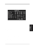
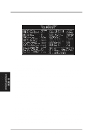
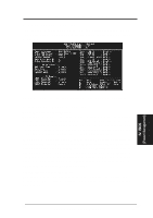
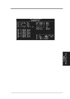
IV. BIOS SOFTWARE Read-Around-Write (Enabled) The default setting of Enabled will increase the execution efficiency of the processor. It allows the processor to execute read commands out of order if there is no dependence between these read and other write commands. 16-bit I/O Recovery Time (1 BUSCLK) Timing for 16-bit ISA cards (leave on default setting of 1 BUSCLK) 8-bit I/O Recovery Time (1 BUSCLK) Timing for 8-bit ISA cards (leave on default setting of 1 BUSCLK) Video Memory Cache Mode (UC) USWC (uncacheable, speculative write combining) is a new cache technology for the video memory of the Pentium Pro processor. It can greatly improve the display speed by caching the display data. You must leave this on the default setting of UC (uncacheable) if your display card cannot support this feature or else your system may not boot. Memory Hole at 15M - 16M (Disabled) Enabling this feature reserves 15MB to 16MB memory address space to ISA expansion cards that specifically require this setting. This makes the memory from 15MB and up unavailable to the system. Expansion cards can only access memory up to 16MB. The default is Disabled. [DRAM and ECC] If all your DRAM modules have parity chips (e.g. 8 chips + 4 parity chips), they are considered 36bits. This motherboard sums the memory per bank and therefore two modules will give 72bits and the following will be displayed: If your DRAM modules do not have parity chips (e.g. 8 chips), they are considered 32bits and the following will be displayed instead: The default of Disabled for Data Integrity will not show memory errors on your monitor. When using parity DRAM modules, you can select ECC (Error Checking and Correcting) to correct 1 bit memory errors that may occur in the memory, otherwise Parity is the default. (See section III for more information on DRAM memory modules.) ...Onboard FDC Controller (Enabled) When enabled, this field allows you to connect your floppy disk drives to the onboard floppy drive connector instead of a separate controller card. If you want to use a different controller card to connect the floppy drives, set this field to Disabled. IV. BIOS (Chipset Features) ASUS KN97-X User's Manual 47
-
 1
1 -
2
-
3
-
4
-
5
-
6
-
7
-
8
-
9
-
10
-
11
-
12
-
13
-
14
-
15
-
16
-
17
-
18
-
19
-
20
-
21
-
22
-
23
-
24
-
25
-
26
-
27
-
28
-
29
-
30
-
31
-
32
-
33
-
34
-
35
-
36
-
37
-
38
-
39
-
40
-
41
-
 42
42 -
 43
43 -
 44
44 -
 45
45 -
 46
46 -
 47
47 -
 48
48 -
 49
49 -
 50
50 -
 51
51 -
 52
52 -
53
-
54
-
55
-
56
-
57
-
58
-
59
-
60
-
61
-
62
-
63
-
64
 |
 |
