Canon MF6530 Service Manual - Page 52
Functional Block Diagram, 1.3 Image Processor PCB - firmware
 |
UPC - 013803056037
View all Canon MF6530 manuals
Add to My Manuals
Save this manual to your list of manuals |
Page 52 highlights
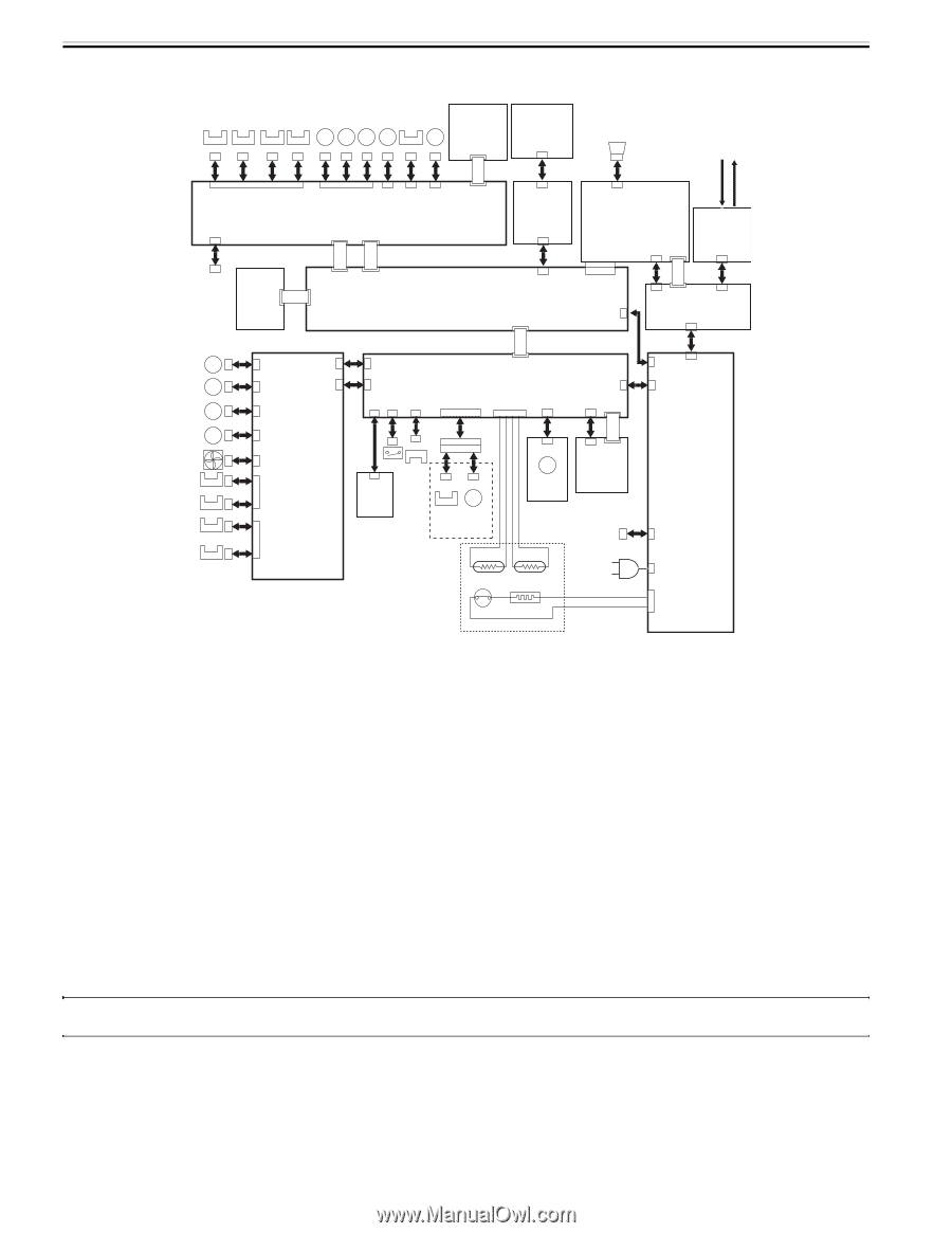
Chapter 2 2.1.2 Functional Block Diagram 0011-3538 J1701 J318 Telephone line Reception Transmission SR2003 SR2001 SL2002 M2001 SR2004 SR2002 SL2003 SL2001 SR401 M401 SL SL SL M M J2006 J2005 J2008 J2007 J2004J2003J2001J2002 J451 Contact snsor J460 PC LAN I/F Speaker*1 J406 J401/ J402 J10/J11 To Power supply PCB Control panel J411 J410 J412 J409 J408 Analog processor PCB J404 J403 Network PCB*2 J1300 J309 J308 Image processor PCB J304 J314 J1203 Modem PCB*1 Mojular jack PCB*1 J1200 J1201 J1202 J1800 J313 J103 J1921 J1924 J1922 NCU PCB*1 J1923 CL1 CL SL1 SL SL5 SL SL2 SL FM1 SR9 J33 SR10 J39 SR12 J36 SR11 J35 J205 J204 J203 J209 J201 J111 J106 J114 J112 J107 J207 Relay PCB J201 J208 J38 SW2 SR5 J2 Humidity sensor J202 *1 : If equipped with fax functions. *2 : If equipped with printer functions. J104 DC controller PCB J108 J113 J110 J900 J903 J902 SL SR1 SL3 Cassette unit (Option) J29 M1 Main motor TH101 TP1 TH102 H1 Fixing unit F-2-2 J103 J105 J102 J30 J31 Scanner unit To analog processor PCB J401/402 J13 J12 J14 Power supply PCB J10/J11 J16 J15 2.1.3 Image Processor PCB 0011-3549 1.function The image processor PCB has the following functions. Control Panel Control Block The control panel control block receives the state of control keys while sending/receiving data in serial communication with the control IC of the control panel PCB. Also, it sends LED and LCD signals to the control panel PCB. Image Processing Control Block - It subjects the digital image data from the analog processor PCB to enlargement/reduction processing, smoothing, and other image processing, thereby converting it to 600x600-dpi image signals (VD0, VD01*, VDO2, VDO2*). - It converts the analog image data from fax communication into 600x600-dpi image signals (VD0, VD01*, VDO2, VDO2*). - It uses a horizontal sync signal (BD0*) as a trigger to send image signals (VD0, VD01*, VDO2, VDO2*) to the laser unit. Smoothing The 600 x 600-dpi image data from the PC is converted into image data equivalent of 1200 x 600 dpi. Sensor Detection It detects the state of each sensor of the reader unit and the ADF. ESS Control It controls the ESS function used to reduce the power consumption while the machine isin standby state. Memory Storage Image data is stored in SDRAM, and is retained for about 1 hr even after the power is removed by the work of the super capacitor mounted on the modem PCB. The system software and various data (e.g., user data, service data) are held by flash ROM. Speaker Control (if equipped with fax functions.) It turns on/off or control the volume of the error sound, key sound, and line monitor sound generated by the speaker. MEMO: The volume of the line monitor or the sound of the key sound or the error sound is adjusted in user mode. 2. Construction The image processor comes in different ROM types/sizes and RAM sizes according to models. The firmware stored in the flash ROM may be either SYSTEM or BOOT. Using the service support tool, the following 3 types of firmware may be upgraded: SYSTEM and BOOT stored in the flash ROM and the firmware stored ion PCL ROM. 2-2
-
 1
1 -
2
-
3
-
4
-
5
-
6
-
7
-
8
-
9
-
10
-
11
-
12
-
13
-
14
-
15
-
16
-
17
-
18
-
19
-
20
-
21
-
22
-
23
-
24
-
25
-
26
-
27
-
28
-
29
-
30
-
31
-
32
-
33
-
34
-
35
-
36
-
37
-
38
-
39
-
40
-
41
-
42
-
43
-
44
-
45
-
46
-
 47
47 -
 48
48 -
 49
49 -
 50
50 -
 51
51 -
 52
52 -
 53
53 -
 54
54 -
 55
55 -
 56
56 -
 57
57 -
58
-
59
-
60
-
61
-
62
-
63
-
64
-
65
-
66
-
67
-
68
-
69
-
70
-
71
-
72
-
73
-
74
-
75
-
76
-
77
-
78
-
79
-
80
-
81
-
82
-
83
-
84
-
85
-
86
-
87
-
88
-
89
-
90
-
91
-
92
-
93
-
94
-
95
-
96
-
97
-
98
-
99
-
100
-
101
-
102
-
103
-
104
-
105
-
106
-
107
-
108
-
109
-
110
-
111
-
112
-
113
-
114
-
115
-
116
-
117
-
118
-
119
-
120
-
121
-
122
-
123
-
124
-
125
-
126
-
127
-
128
-
129
-
130
-
131
-
132
-
133
-
134
-
135
-
136
-
137
-
138
-
139
-
140
-
141
-
142
-
143
-
144
-
145
-
146
-
147
-
148
-
149
-
150
-
151
-
152
-
153
-
154
-
155
-
156
-
157
-
158
-
159
-
160
-
161
-
162
-
163
-
164
-
165
-
166
-
167
-
168
-
169
-
170
-
171
-
172
-
173
-
174
-
175
-
176
-
177
-
178
-
179
-
180
-
181
-
182
-
183
-
184
-
185
-
186
-
187
-
188
-
189
-
190
-
191
-
192
-
193
-
194
-
195
-
196
-
197
-
198
-
199
-
200
-
201
-
202
-
203
-
204
-
205
-
206
-
207
-
208
-
209
-
210
-
211
-
212
-
213
-
214
-
215
-
216
-
217
-
218
-
219
-
220
-
221
-
222
-
223
-
224
-
225
-
226
-
227
-
228
-
229
-
230
-
231
-
232
-
233
-
234
-
235
-
236
-
237
-
238
-
239
-
240
-
241
-
242
-
243
-
244
-
245
-
246
-
247
-
248
-
249
-
250
 |
 |