Compaq dc7100 HP Compaq dc71xx and dx61xx Series Business Desktop Computers Te - Page 90
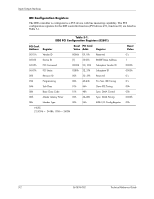
Table 5-3., Pin IDE PATA Connector Pinout, Signal, Description
 |
View all Compaq dc7100 manuals
Add to My Manuals
Save this manual to your list of manuals |
Page 90 highlights
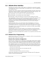
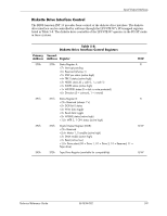
Input/Output Interfaces Table 5-3. 40-Pin IDE (PATA) Connector Pinout Pin Signal Description Pin Signal Description 1 RESET- Reset 21 DRQ DMA Request 2 GND Ground 22 GND Ground 3 DD7 Data Bit 23 IOW- I/O Write [1] 4 DD8 Data Bit 24 GND Ground 5 DD6 Data Bit 25 IOR- I/O Read [2] 6 DD9 Data Bit 26 GND Ground 7 DD5 Data Bit 27 IORDY I/O Channel Ready [3] 8 DD10 Data Bit 28 CSEL Cable Select 9 DD4 Data Bit 29 DAK- DMA Acknowledge 10 DD11 Data Bit 30 GND Ground 11 DD3 Data Bit 31 IRQn Interrupt Request [4] 12 DD12 Data Bit 32 IO16- 16-bit I/O 13 DD2 Data Bit 33 DA1 Address 1 14 DD13 Data Bit 34 DSKPDIAG Pass Diagnostics 15 DD1 Data Bit 35 DA0 Address 0 16 DD14 Data Bit 36 DA2 Address 2 17 DD0 Data Bit 37 CS0- Chip Select 18 DD15 Data Bit 38 CS1- Chip Select 19 GND Ground 39 HDACTIVE- Drive Active (front panel LED) [5] 20 -- Key 40 GND Ground NOTES: [1] On UATA/33 and higher modes, re-defined as STOP. [2] On UATA/33 and higher mode reads, re-defined as DMARDY-. On UATA/33 and higher mode writes, re-defined as STROBE. [3] On UATA/33 and higher mode reads, re-defined as STROBE-. On UATA/33 and higher mode writes, re-defined as DMARDY-. [4] Primary connector wired to IRQ14, secondary connector wired to IRQ15. [5] Pin 39 is used for spindle sync and drive activity (becomes SPSYNC/DACT-) when synchronous drives are connected. 5-4 361834-002 Technical Reference Guide
-
 1
1 -
2
-
3
-
4
-
5
-
6
-
7
-
8
-
9
-
10
-
11
-
12
-
13
-
14
-
15
-
16
-
17
-
18
-
19
-
20
-
21
-
22
-
23
-
24
-
25
-
26
-
27
-
28
-
29
-
30
-
31
-
32
-
33
-
34
-
35
-
36
-
37
-
38
-
39
-
40
-
41
-
42
-
43
-
44
-
45
-
46
-
47
-
48
-
49
-
50
-
51
-
52
-
53
-
54
-
55
-
56
-
57
-
58
-
59
-
60
-
61
-
62
-
63
-
64
-
65
-
66
-
67
-
68
-
69
-
70
-
71
-
72
-
73
-
74
-
75
-
76
-
77
-
78
-
79
-
80
-
81
-
82
-
83
-
84
-
 85
85 -
 86
86 -
 87
87 -
 88
88 -
 89
89 -
 90
90 -
 91
91 -
 92
92 -
 93
93 -
 94
94 -
 95
95 -
96
-
97
-
98
-
99
-
100
-
101
-
102
-
103
-
104
-
105
-
106
-
107
-
108
-
109
-
110
-
111
-
112
-
113
-
114
-
115
-
116
-
117
-
118
-
119
-
120
-
121
-
122
-
123
-
124
-
125
-
126
-
127
-
128
-
129
-
130
-
131
-
132
-
133
-
134
-
135
-
136
-
137
-
138
-
139
-
140
-
141
-
142
-
143
-
144
-
145
-
146
-
147
-
148
-
149
-
150
-
151
-
152
-
153
-
154
-
155
-
156
-
157
-
158
-
159
-
160
-
161
-
162
-
163
-
164
-
165
-
166
-
167
-
168
-
169
-
170
-
171
-
172
-
173
-
174
-
175
-
176
-
177
-
178
-
179
-
180
-
181
-
182
-
183
-
184
-
185
-
186
-
187
-
188
-
189
-
190
-
191
-
192
-
193
-
194
-
195
-
196
-
197
-
198
-
199
-
200
-
201
-
202
-
203
-
204
-
205
-
206
-
207
-
208
-
209
-
210
-
211
-
212
 |
 |