Intel D925XHY D925XHY Technical Product Specification - Page 43

Technical Reference

Page 43 highlights

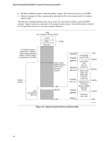
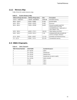
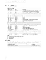
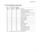
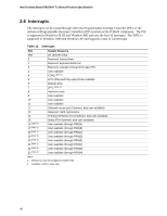
2 Technical Reference What This Chapter Contains 2.1 Introduction ...43 2.2 Memory Resources ...43 2.3 DMA Channels ...45 2.4 Fixed I/O Map...46 2.5 PCI Configuration Space Map 47 2.6 Interrupts ...48 2.7 PCI Conventional Interrupt Routing Map 49 2.8 Connectors...50 2.9 Jumper Block ...61 2.10 Mechanical Considerations 62 2.11 Electrical Considerations 64 2.12 Thermal Considerations 66 2.13 Reliability...68 2.14 Environmental ...69 2.15 Regulatory Compliance 70 2.1 Introduction Sections 2.2 - 2.6 contain several standalone tables. Table 8 describes the system memory map, Table 9 lists the DMA channels, Table 10 shows the I/O map, Table 11 defines the PCI Conventional bus configuration space map, and Table 12 describes the interrupts. The remaining sections in this chapter are introduced by text found with their respective section headings. 2.2 Memory Resources 2.2.1 Addressable Memory The board utilizes 4 GB of addressable system memory. Typically the address space that is allocated for PCI Conventional bus add-in cards, PCI Express configuration space, BIOS (firmware hub), and chipset overhead resides above the top of DRAM (total system memory). On a system that has 4 GB of system memory installed, it is not possible to use all of the installed memory due to system address space being allocated for other system critical functions. These functions include the following: • BIOS/firmware hub (2 MB) • Local APIC (19 MB) • Digital Media Interface (40 MB) • Front side bus interrupts (17 MB) • PCI Express configuration space (256 MB) 43

  • 1
  • 2
  • 3
  • 4
  • 5
  • 6
  • 7
  • 8
  • 9
  • 10
  • 11
  • 12
  • 13
  • 14
  • 15
  • 16
  • 17
  • 18
  • 19
  • 20
  • 21
  • 22
  • 23
  • 24
  • 25
  • 26
  • 27
  • 28
  • 29
  • 30
  • 31
  • 32
  • 33
  • 34
  • 35
  • 36
  • 37
  • 38
  • 39
  • 40
  • 41
  • 42
  • 43
  • 44
  • 45
  • 46
  • 47
  • 48
  • 49
  • 50
  • 51
  • 52
  • 53
  • 54
  • 55
  • 56
  • 57
  • 58
  • 59
  • 60
  • 61
  • 62
  • 63
  • 64
  • 65
  • 66
  • 67
  • 68
  • 69
  • 70
  • 71
  • 72
  • 73
  • 74
  • 75
  • 76
  • 77
  • 78
  • 79
  • 80
  • 81
  • 82
  • 83
  • 84
  • 85
  • 86
  • 87
  • 88
  • 89
  • 90
  • 91
  • 92

43
2 Technical Reference
What This Chapter Contains
2.1
Introduction
..................................................................................................................
43
2.2
Memory Resources
......................................................................................................
43
2.3
DMA Channels
.............................................................................................................
45
2.4
Fixed I/O Map
...............................................................................................................
46
2.5
PCI Configuration Space Map
......................................................................................
47
2.6
Interrupts
......................................................................................................................
48
2.7
PCI Conventional Interrupt Routing Map
.....................................................................
49
2.8
Connectors
...................................................................................................................
50
2.9
Jumper Block
...............................................................................................................
61
2.10
Mechanical Considerations
..........................................................................................
62
2.11
Electrical Considerations
..............................................................................................
64
2.12
Thermal Considerations
...............................................................................................
66
2.13
Reliability
......................................................................................................................
68
2.14
Environmental
..............................................................................................................
69
2.15
Regulatory Compliance
................................................................................................
70
2.1 Introduction
Sections 2.2 - 2.6 contain several standalone tables.
Table 8 describes the system memory map,
Table 9 lists the DMA channels, Table 10 shows the I/O map, Table 11 defines the PCI
Conventional bus configuration space map, and Table 12 describes the interrupts.
The remaining
sections in this chapter are introduced by text found with their respective section headings.
2.2 Memory Resources
2.2.1
Addressable Memory
The board utilizes 4 GB of addressable system memory.
Typically the address space that is
allocated for PCI Conventional bus add-in cards, PCI Express configuration space, BIOS (firmware
hub), and chipset overhead resides above the top of DRAM (total system memory).
On a system
that has 4 GB of system memory installed, it is not possible to use all of the installed memory due
to system address space being allocated for other system critical functions.
These functions include
the following:
BIOS/firmware hub (2 MB)
Local APIC (19 MB)
Digital Media Interface (40 MB)
Front side bus interrupts (17 MB)
PCI Express configuration space (256 MB)