Intel D925XHY D925XHY Technical Product Specification - Page 46
Fixed I/O Map
 |
View all Intel D925XHY manuals
Add to My Manuals
Save this manual to your list of manuals |
Page 46 highlights
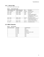
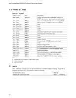
Intel Desktop Board D925XHY Technical Product Specification 2.4 Fixed I/O Map Table 10. I/O Map Address (hex) 0000 - 00FF Size 256 bytes 0170 - 0177 01F0 - 01F7 0228 - 022F (Note 1) 0278 - 027F (Note 1) 02E8 - 02EF (Note 1) 02F8 - 02FF (Note 1) 0374 - 0377 0377, bits 6:0 0378 - 037F 03E8 - 03EF 03F0 - 03F5 03F4 - 03F7 03F8 - 03FF 04D0 - 04D1 LPTn + 400 0CF8 - 0CFB (Note 2) 0CF9 (Note 3) 0CFC - 0CFF FFA0 - FFA7 FFA8 - FFAF 8 bytes 8 bytes 8 bytes 8 bytes 8 bytes 8 bytes 4 bytes 7 bits 8 bytes 8 bytes 6 bytes 1 byte 8 bytes 2 bytes 8 bytes 4 bytes 1 byte 4 bytes 8 bytes 8 bytes Description Used by the Desktop Board D925XHY. Refer to the ICH6-R data sheet for dynamic addressing information. Secondary Parallel ATA IDE channel command block Primary Parallel ATA IDE channel command block LPT3 LPT2 COM4 COM2 Secondary Parallel ATA IDE channel control block Secondary IDE channel status port LPT1 COM3 Diskette channel Primary Parallel ATA IDE channel control block COM1 Edge/level triggered PIC ECP port, LPTn base address + 400h PCI Conventional bus configuration address register Reset control register PCI Conventional bus configuration data register Primary Parallel ATA IDE bus master registers Secondary Parallel ATA IDE bus master registers Notes: 1. Default, but can be changed to another address range. 2. Dword access only. 3. Byte access only. NOTE Some additional I/O addresses are not available due to ICH6-R address aliasing. The ICH6-R data sheet provides more information on address aliasing. For information about Obtaining the ICH6-R data sheet Refer to Section 1.2 on page 15 46
-
 1
1 -
2
-
3
-
4
-
5
-
6
-
7
-
8
-
9
-
10
-
11
-
12
-
13
-
14
-
15
-
16
-
17
-
18
-
19
-
20
-
21
-
22
-
23
-
24
-
25
-
26
-
27
-
28
-
29
-
30
-
31
-
32
-
33
-
34
-
35
-
36
-
37
-
38
-
39
-
40
-
 41
41 -
 42
42 -
 43
43 -
 44
44 -
 45
45 -
 46
46 -
 47
47 -
 48
48 -
 49
49 -
 50
50 -
 51
51 -
52
-
53
-
54
-
55
-
56
-
57
-
58
-
59
-
60
-
61
-
62
-
63
-
64
-
65
-
66
-
67
-
68
-
69
-
70
-
71
-
72
-
73
-
74
-
75
-
76
-
77
-
78
-
79
-
80
-
81
-
82
-
83
-
84
-
85
-
86
-
87
-
88
-
89
-
90
-
91
-
92
 |
 |
