AMD AXDA3200DKV4E Data Sheet - Page 14

QuantiSpeed™ Architecture Summary, Overview, - voltage
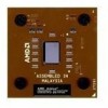
Page 14 highlights

Preliminary Information AMD Athlon™ XP Processor Model 10 Data Sheet 26237C-May 2003 The features of the AMD Athlon XP processor model 10 are QuantiSpeed™ architecture, 640 Kbytes of total, highperformance, full-speed, on-chip cache, an advanced 400 frontside bus (FSB) with a 3.2-Gigabyte per second system bus, or an advanced 333 FSB with a 2.7-Gigabyte per second system bus, and 3DNow!™ Professional technology. The AMD Athlon system bus combines the latest technological advances, such as point-to-point topology, source-synchronous packet-based transfers, and low-voltage signaling to provide an extremely powerful, scalable bus for an x86 processor. The AMD Athlon XP processor model 10 is binary-compatible with existing x86 software and backwards compatible with applications optimized for MMX™, SSE, and 3DNow! technology. Using a data format and single-instruction multiple-data (SIMD) operations based on the MMX instruction model, the AMD Athlon XP processor model 10 can produce as many as four, 32-bit, single-precision floating-point results per clock cycle. The 3DNow! Professional technology implemented in the AMD Athlon XP processor model 10 includes new integer multimedia instructions and software-directed data movement instructions for optimizing such applications as digital content creation and streaming video for the internet, as well as new instructions for digital signal processing (DSP) and communications applications. 1.1 QuantiSpeed™ Architecture Summary The following features summarize the AMD Athlon XP processor model 10 QuantiSpeed architecture: ■ An advanced nine-issue, superpipelined, superscalar x86 processor microarchitecture designed for increased instructions per cycle (IPC) and high clock frequencies ■ Fully pipelined floating-point unit that executes all x87 (floating-point), MMX, SSE and 3DNow! instructions ■ Hardware data pre-fetch that increases and optimizes performance on high-end software applications utilizing high-bandwidth system capabilities ■ Advanced two-level translation look-aside buffer (TLB) structures for both enhanced data and instruction address translation. The AMD Athlon XP processor model 10 with QuantiSpeed architecture incorporates three TLB optimizations: the L1 DTLB increases from 32 to 40 entries, the L2 ITLB and L2 DTLB both use exclusive architecture, and the TLB entries can be speculatively loaded. 2 Overview Chapter 1

  • 1
  • 2
  • 3
  • 4
  • 5
  • 6
  • 7
  • 8
  • 9
  • 10
  • 11
  • 12
  • 13
  • 14
  • 15
  • 16
  • 17
  • 18
  • 19
  • 20
  • 21
  • 22
  • 23
  • 24
  • 25
  • 26
  • 27
  • 28
  • 29
  • 30
  • 31
  • 32
  • 33
  • 34
  • 35
  • 36
  • 37
  • 38
  • 39
  • 40
  • 41
  • 42
  • 43
  • 44
  • 45
  • 46
  • 47
  • 48
  • 49
  • 50
  • 51
  • 52
  • 53
  • 54
  • 55
  • 56
  • 57
  • 58
  • 59
  • 60
  • 61
  • 62
  • 63
  • 64
  • 65
  • 66
  • 67
  • 68
  • 69
  • 70
  • 71
  • 72
  • 73
  • 74
  • 75
  • 76
  • 77
  • 78
  • 79
  • 80
  • 81
  • 82
  • 83
  • 84
  • 85
  • 86
  • 87
  • 88
  • 89
  • 90
  • 91
  • 92
  • 93
  • 94
  • 95
  • 96
  • 97
  • 98
  • 99
  • 100
  • 101
  • 102
  • 103
  • 104

2
Overview
Chapter 1
AMD Athlon™ XP Processor Model 10 Data Sheet
26237C—May 2003
Preliminary Information
The features of the AMD Athlon XP processor model 10 are
QuantiSpeed™ architecture, 640 Kbytes of total, high-
performance, full-speed, on-chip cache, an advanced 400 front-
side bus (FSB) with a 3.2-Gigabyte per second system bus, or an
advanced 333 FSB with a 2.7-Gigabyte per second system bus,
and 3DNow!™ Professional technology. The AMD Athlon system
bus combines the latest technological advances, such as
point-to-point topology, source-synchronous packet-based
transfers, and low-voltage signaling to provide an extremely
powerful, scalable bus for an x86 processor.
The AMD Athlon XP processor model 10 is binary-compatible
with existing x86 software and backwards compatible with
applications optimized for MMX™, SSE, and 3DNow! technology.
Using a data format and single-instruction multiple-data (SIMD)
operations based on the MMX instruction model, the
AMD Athlon XP processor model 10 can produce as many as four,
32-bit, single-precision floating-point results per clock cycle. The
3DNow! Professional technology implemented in the
AMD Athlon XP processor model 10 includes new integer
multimedia instructions and software-directed data movement
instructions for optimizing such applications as digital content
creation and streaming video for the internet, as well as new
instructions for digital signal processing (DSP) and
communications applications.
1.1
QuantiSpeed™ Architecture Summary
The following features summarize the AMD Athlon XP
processor model 10 QuantiSpeed architecture:
An advanced nine-issue, superpipelined, superscalar x86
processor
microarchitecture
designed
for
increased
instructions per cycle (IPC) and high clock frequencies
Fully pipelined floating-point unit that executes all x87
(floating-point), MMX
,
SSE and 3DNow! instructions
Hardware data pre-fetch that increases and optimizes
performance on high-end software applications utilizing
high-bandwidth system capabilities
Advanced two-level translation look-aside buffer (TLB)
structures for both enhanced data and instruction address
translation. The AMD Athlon XP processor model 10 with
QuantiSpeed
architecture
incorporates
three
TLB
optimizations: the L1 DTLB increases from 32 to 40 entries,
the L2 ITLB and L2 DTLB both use exclusive architecture,
and the TLB entries can be speculatively loaded.