AMD AXDA3200DKV4E Data Sheet - Page 86

FID[3:0] Pins, FID[3] Y3, and FID[0] W1 are
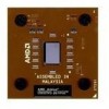
Page 86 highlights

Preliminary Information AMD Athlon™ XP Processor Model 10 Data Sheet 26237C-May 2003 FID[3:0] Pins 74 FID[3] (Y3), FID[2] (Y1), FID[1] (W3), and FID[0] (W1) are the 4-bit processor clock-to-SYSCLK ratio. Table 25 describes the encodings of the clock multipliers on FID[3:0]. Table 25. FID[3:0] Clock Multiplier Encodings FID[3:0]2 Processor Clock to SYSCLK Frequency Ratio 0000 11 0001 11.5 0010 12 0011 ≥ 12.51 0100 5 0101 5.5 0110 6 0111 6.5 1000 7 1001 7.5 1010 8 1011 8.5 1100 9 1101 9.5 1110 10 1111 10.5 Notes: 1. All ratios greater than or equal to 12.5x have the same FID[3:0] code of 0011b, which causes the SIP configuration for all ratios of 12.5x or greater to be the same. 2. BIOS initializes the CLK_Ctl MSR during the POST routine. This CLK_Ctl setting is used with all FID combinations and selects a Halt disconnect divisor and a Stop Grant disconnect divisor. For more information, refer to the AMD Athlon™ and AMD Duron™ Processors BIOS, Software, and Debug Developers Guide, order# 21656. The FID[3:0] signals are open-drain processor outputs that are pulled High on the motherboard and sampled by the chipset to determine the SIP (serial initialization packet) that is sent to the processor. The FID[3:0] signals are valid after PWROK is asserted. The FID[3:0]signals must not be sampled until they become valid. See the AMD Athlon™ and AMD Duron™ System Bus Specification, order# 21902 for more information about Serialization Initialization Packets and SIP protocol. The processor FID[3:0] outputs are open-drain and 2.5-V tolerant. To prevent damage to the processor, do not pull these Pin Descriptions Chapter 11

  • 1
  • 2
  • 3
  • 4
  • 5
  • 6
  • 7
  • 8
  • 9
  • 10
  • 11
  • 12
  • 13
  • 14
  • 15
  • 16
  • 17
  • 18
  • 19
  • 20
  • 21
  • 22
  • 23
  • 24
  • 25
  • 26
  • 27
  • 28
  • 29
  • 30
  • 31
  • 32
  • 33
  • 34
  • 35
  • 36
  • 37
  • 38
  • 39
  • 40
  • 41
  • 42
  • 43
  • 44
  • 45
  • 46
  • 47
  • 48
  • 49
  • 50
  • 51
  • 52
  • 53
  • 54
  • 55
  • 56
  • 57
  • 58
  • 59
  • 60
  • 61
  • 62
  • 63
  • 64
  • 65
  • 66
  • 67
  • 68
  • 69
  • 70
  • 71
  • 72
  • 73
  • 74
  • 75
  • 76
  • 77
  • 78
  • 79
  • 80
  • 81
  • 82
  • 83
  • 84
  • 85
  • 86
  • 87
  • 88
  • 89
  • 90
  • 91
  • 92
  • 93
  • 94
  • 95
  • 96
  • 97
  • 98
  • 99
  • 100
  • 101
  • 102
  • 103
  • 104

74
Pin Descriptions
Chapter 11
AMD Athlon™ XP Processor Model 10 Data Sheet
26237C—May 2003
Preliminary Information
FID[3:0] Pins
FID[3] (Y3), FID[2] (Y1), FID[1] (W3), and FID[0] (W1) are the
4-bit processor clock-to-SYSCLK ratio.
Table 25 describes the encodings of the clock multipliers on
FID[3:0].
The FID[3:0] signals are open-drain processor outputs that are
pulled High on the motherboard and sampled by the chipset to
determine the SIP (serial initialization packet) that is sent to
the processor. The FID[3:0] signals are valid after PWROK is
asserted. The FID[3:0]signals must not be sampled until they
become valid. See the
AMD Athlon™ and AMD Duron™ System
Bus Specification
, order# 21902 for more information about
Serialization Initialization Packets and SIP protocol.
The processor FID[3:0] outputs are open-drain and 2.5-V
tolerant. To prevent damage to the processor, do not pull these
Table 25.
FID[3:0] Clock Multiplier Encodings
FID[3:0]
2
Processor Clock to SYSCLK Frequency Ratio
0000
11
0001
11.5
0010
12
0011
12.5
1
0100
5
0101
5.5
0110
6
0111
6.5
1000
7
1001
7.5
1010
8
1011
8.5
1100
9
1101
9.5
1110
10
1111
10.5
Notes:
1.
All ratios greater than or equal to 12.5x have the same FID[3:0] code of 0011b, which causes
the SIP configuration for all ratios of 12.5x or greater to be the same.
2.
BIOS initializes the CLK_Ctl MSR during the POST routine. This CLK_Ctl setting is used with all
FID combinations and selects a Halt disconnect divisor and a Stop Grant disconnect divisor.
For more information, refer to the
AMD Athlon™ and AMD Duron™ Processors BIOS,
Software, and Debug Developers Guide
, order# 21656.