Foxconn A7GM-S English Manual. - Page 41
► Memory Speed Mode, ► Memory Speed Adjust, ► DRAM Timing Mode, ► tCL CAS Latency, ► tRCD RAS-to-CAS - am2
 |
View all Foxconn A7GM-S manuals
Add to My Manuals
Save this manual to your list of manuals |
Page 41 highlights
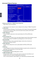
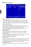
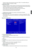
DRAM Timing Configuration CMOS Setup Utility - Copyright (C) 1985-2006, American Megatrends, Inc. DRAM Timing Configuration DRAM Timing Configuration Help Item Memory Speed Mode [Auto] DRAM Timing Mode [Auto] Options Auto Limit Manual 3 Move Enter:Select +/-/:Value F10:Save ESC:Exit F1:General Help F9:Optimized Defaults ► Memory Speed Mode This item is used to enable/disable provision of DRAM timing by SPD device. The Serial Presence Detect (SPD) device is a small EEPROM chip, mounted on a DDR2 memory module. It contains important information about the module's speed, size, addressing mode and various other parameters, so that the motherboard memory controller (chipset) can better access the memory device. Select [Auto] for SPD enable mode. Select [Limit], the DRAM speed will not exceed the specified value listed in the "Memory Speed Adjust" item. If SPD value is faster than "Memory Speed Adjust" value, it will run at the specified "Memory Speed Adjust" speed. Otherwise, SPD value is selected. Select [Manual], then DRAM speed is manually selected according to the set value of "Memory Speed Adjust". ► Memory Speed Adjust This item will appear only when the "Memory Speed Mode" is set to [Limit] or [Manual]. The available settings are : [400MHz], [533MHz], [667MHz], [800MHz], [1066MHz]. ► DRAM Timing Mode When both DCTs (DRAM controller) are enabled in unganged mode, BIOS must initialize the frequency of each DCT in order, you also can configure the timings manually. Settings are : [Auto], [DCT 0], [DCT1], [Both]. [DCT 1] and [Both] will appear only in AM2+ CPU. ► tCL (CAS Latency) The number of memory clocks it takes a DRAM to return data after the read CAS_L is asserted depends on the memory clock frequency. The value that BIOS programs into the memory controller is a function of the target clock frequency. The target clock frequency is determined from the supported CAS latencies at given clock frequencies of each DIMM. ► tRCD (RAS-to-CAS Delay) This item allows you to select a delay time (in clock cycles) between the CAS# and RAS# strobe signals. 34
-
 1
1 -
2
-
3
-
4
-
5
-
6
-
7
-
8
-
9
-
10
-
11
-
12
-
13
-
14
-
15
-
16
-
17
-
18
-
19
-
20
-
21
-
22
-
23
-
24
-
25
-
26
-
27
-
28
-
29
-
30
-
31
-
32
-
33
-
34
-
35
-
 36
36 -
 37
37 -
 38
38 -
 39
39 -
 40
40 -
 41
41 -
 42
42 -
 43
43 -
 44
44 -
 45
45 -
 46
46 -
47
-
48
-
49
-
50
-
51
-
52
-
53
-
54
-
55
-
56
-
57
-
58
-
59
-
60
-
61
-
62
-
63
-
64
-
65
-
66
-
67
-
68
-
69
-
70
-
71
-
72
-
73
-
74
-
75
-
76
-
77
-
78
-
79
-
80
-
81
-
82
-
83
-
84
-
85
-
86
-
87
-
88
-
89
-
90
-
91
-
92
-
93
-
94
-
95
-
96
-
97
-
98
-
99
-
100
-
101
-
102
-
103
-
104
-
105
-
106
-
107
 |
 |