Intel DG33TL Product Specification - Page 81
Table 41. Lead-Free Board Markings
 |
View all Intel DG33TL manuals
Add to My Manuals
Save this manual to your list of manuals |
Page 81 highlights
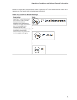
Regulatory Compliance and Battery Disposal Information Table 41 shows the various forms of the "Lead-Free 2nd Level Interconnect" mark as it appears on the board and accompanying collateral. Table 41. Lead-Free Board Markings Description Lead-Free 2nd Level Interconnect: This symbol is used to identify electrical and electronic assemblies and components in which the lead (Pb) concentration level in the desktop board substrate and the solder connections from the board to the components (second-level interconnect) is not greater than 0.1% by weight (1000 ppm). Mark or or 81
-
 1
1 -
2
-
3
-
4
-
5
-
6
-
7
-
8
-
9
-
10
-
11
-
12
-
13
-
14
-
15
-
16
-
17
-
18
-
19
-
20
-
21
-
22
-
23
-
24
-
25
-
26
-
27
-
28
-
29
-
30
-
31
-
32
-
33
-
34
-
35
-
36
-
37
-
38
-
39
-
40
-
41
-
42
-
43
-
44
-
45
-
46
-
47
-
48
-
49
-
50
-
51
-
52
-
53
-
54
-
55
-
56
-
57
-
58
-
59
-
60
-
61
-
62
-
63
-
64
-
65
-
66
-
67
-
68
-
69
-
70
-
71
-
72
-
73
-
74
-
75
-
 76
76 -
 77
77 -
 78
78 -
 79
79 -
 80
80 -
 81
81 -
 82
82 -
 83
83 -
 84
84 -
 85
85 -
 86
86 -
87
-
88
 |
 |
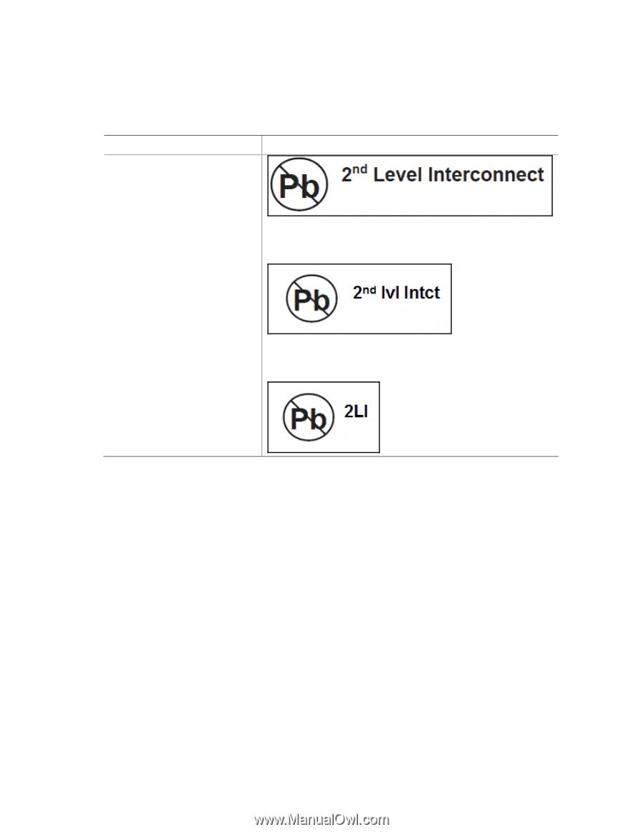
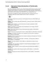
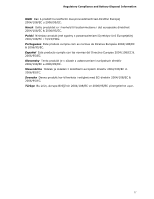
Regulatory Compliance and Battery Disposal Information
81
Table 41 shows the various forms of the “Lead-Free 2
nd
Level Interconnect” mark as it
appears on the board and accompanying collateral.
Table 41. Lead-Free Board Markings
Description
Mark
Lead-Free 2
nd
Level Interconnect:
This symbol is used to identify
electrical and electronic
assemblies and components in
which the lead (Pb) concentration
level in the desktop board
substrate and the solder
connections from the board to the
components (second-level
interconnect) is not greater than
0.1% by weight (1000 ppm).
or
or