Sony MZ-NF810CK Service Manual
Sony MZ-NF810CK Manual
 |
View all Sony MZ-NF810CK manuals
Add to My Manuals
Save this manual to your list of manuals |
Sony MZ-NF810CK manual content summary:
- Sony MZ-NF810CK | Service Manual - Page 1
are trademarks or registered trademarks of Intel Corporation. Model Name Using Similar Mechanism Mechanism Type Optical Pick-up Name MZ-R410 MT-MZN710-177 LCX-5R SPECIFICATIONS MD recorder Audio playing system MiniDisc digital audio system Laser diode properties Material: GaAlAs Wavelength - Sony MZ-NF810CK | Service Manual - Page 2
Approx. 108 g (3.8 oz) the recorder only 1)The LINE IN (OPTICAL) jack is used to connect either a digital (optical) cable or a line (analog) cable. 2)The i jack connects either headphones/ earphones or a line cable. 3)Measured in accordance with JEITA. Car kit Car connecting pack Frequency response - Sony MZ-NF810CK | Service Manual - Page 3
MZ-NF810/NF810CK CAUTION Use of controls or adjustments or performance of procedures other than those specified herein may result in hazardous radiation exposure. On power sources • Use house current, nickel metal hydride rechargeable battery, LR6 (size AA) battery, or car battery. • For use in - Sony MZ-NF810CK | Service Manual - Page 4
MZ-NF810/NF810CK SECTION 1 SERVICING software are required in order to use the SonicStage software for the Net MD (supports Web registration and EMD services Windows Media Player (version 7.0 or trouble-free operation on all computers that satisfy the system requirements. • We do not ensure trouble - Sony MZ-NF810CK | Service Manual - Page 5
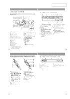
MZ-NF810/NF810CK This section is extracted from instruction manual. Looking at controls The recorder 1 2 3 4 5 6 7 8 9 q; qa qs qg qd qf qh qj qk w; ql A x • CANCEL/CHG button B Display window C Battery compartment D GROUP button E REC (record) switch F Terminals for attaching dry battery - Sony MZ-NF810CK | Service Manual - Page 6
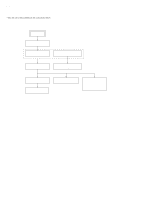
MZ-NF810/NF810CK • This set can be disassembled in the order shown below. 3-1. Disassembly Flow SECTION 3 DISASSEMBLY SET CASE (LOWER) MAIN BOARD, BATTERY CASE In order to remove mechanism deck (MT-MZN710-177) , please remove MAIN board and upper panel section. PANEL (UPPER) SECTION MECHANISM - Sony MZ-NF810CK | Service Manual - Page 7
order given. 3-2. Case (Lower) MZ-NF810/NF810CK 6 two screws (M1.4) 4 two screws (M1.4) 2 claw 7 Remove the case (lower) in the direction of the arrow. 5 screw (M1.4) battery lid 1 Open the battery case lid. 3 Remove the battery case lid. 3-3. MAIN Board, Battery Case 2 Remove the solder of - Sony MZ-NF810CK | Service Manual - Page 8
MZ-NF810/NF810CK 3-4. Panel (Upper) Section 3 two screws (M1.4) 1 flexible board (CN871) 5 upper panel section set chassis assy 4 two screws (M1.4) torsion spring (pop up-L) 6 torsion spring (pop - Sony MZ-NF810CK | Service Manual - Page 9
3-6. Mechanism Deck (MT-MZN710-177) MZ-NF810/NF810CK 1 two step screws (MD) 3 mechanism deck (MT-MZN710-177) 4 set chassis assy 2 9 - Sony MZ-NF810CK | Service Manual - Page 10
MZ-NF810/NF810CK 3-7. OP Service Assy (LCX-5R) 1 washer (0.8-2.5) 3 screw (M1.4) 4 rack spring 2 gear (SA) 5 screw (M1.4) 6 thrust detent spring 8 Pull off lead screw. 7 9 Opening the over write head toward the direction A, remove the OP service assy (LCX-5R) toward the direction B. B Note: - Sony MZ-NF810CK | Service Manual - Page 11
3-8. Holder Assy MZ-NF810/NF810CK 4 holder assy 2 Open the holder assy. 1 convex portion 3 boss 3 boss 3-9. DC Motor (Sled) (M602) 2 washer (0.8-2.5) 3 gear (SA) 4 two screws (M1.4) 5 DC motor (sled) (M602) 1 Remove six solders of the motor flexible board. 11 - Sony MZ-NF810CK | Service Manual - Page 12
MZ-NF810/NF810CK 3-10. DC Motor (Over Write Head Up/Down) (M603), DC SSM18B Motor (Spindle) (M601) 1 Remove six solders of the motor flexible board. 8 three tapping screws 2 - Sony MZ-NF810CK | Service Manual - Page 13
SECTION 4 TEST MODE MZ-NF810/NF810CK Outline • This set provides the Overall adjustment mode executed in order. If a fault is found, the system displays its location. Also, the manual mode allows each individual adjustment to be automatically adjusted. • Operation in the test mode is performed - Sony MZ-NF810CK | Service Manual - Page 14
MZ-NF810/NF810CK Configuration of Test Mode [Test Mode $Display Check Mode%] Press the > or [VOL +] key [Manual Mode] Press the xCANCEL/CHG key [ , the adjustment in this mode is not executed. However, the Manual mode is used to clear the memory, power supply adjustment, and laser power check - Sony MZ-NF810CK | Service Manual - Page 15
MZ-NF810/NF810CK 5. The power mode (item number 700's), only the item is displayed. 6. Quit the manual mode, and press the xCANCEL/CHG key to return to the test mode recording time is recorded as a guideline of how long the optical pick-up has been used, and by comparing it with the total recording - Sony MZ-NF810CK | Service Manual - Page 16
MZ-NF810/NF810CK • Description of error indication codes Problem battery Offset error Focus error ABCD offset error Tracking error Offset error X1 tracking error Offset error MD errors before the last. Total recording time Reset the Error Display Code After servicing, reset the error display code. - Sony MZ-NF810CK | Service Manual - Page 17
MZ-NF810/NF810CK Sound Skip Check Result Display Mode This set can display the count of errors that occurred during the recording/playing for by one, then if the [REC] key is pressed, the display in the record mode appears. When the [REC] key is pressed, total error count is displayed on - Sony MZ-NF810CK | Service Manual - Page 18
MZ-NF810/NF810CK SECTION 5 ELECTRICAL ADJUSTMENTS Outline • In this set, automatic adjustment of CD and MO can be per- formed by entering the test mode. However, before starting automatic adjustment, the memory clear, power supply adjustment, and laser power check must be performed in the manual - Sony MZ-NF810CK | Service Manual - Page 19
MZ-NF810/NF810CK • Adjustment Method of VC1_LOW (PB) (item number: 741) Remote commander LCD display 741 VC1 L ** **: Adjusted value 1. Connect a digital voltmeter to the TP1928 (VCO1) on the - Sony MZ-NF810CK | Service Manual - Page 20
MZ-NF810/NF810CK • Adjustment Method of REG3_LOW2 (item number: 748) Remote commander LCD display 748 REG3L2 ** **: Adjusted value 1. Connect a digital voltmeter to the TP1907 (REGO3) on the MAIN - Sony MZ-NF810CK | Service Manual - Page 21
MZ-NF810/NF810CK • Adjustment Method of CHGV_LOW (item number: 755) Remote commander LCD display 755 ChgV L ** **: Adjusted value Note: Remove the rechargeable battery. 1. Connect a digital voltmeter to the BATT+ on the MAIN board, and adjust [VOL +] key (voltage up) or [VOL --] key (voltage down) - Sony MZ-NF810CK | Service Manual - Page 22
MZ-NF810/NF810CK Adjustment/checking and Connection Location: MAIN BOARD (SIDE B) BATT- (GND) TP1905(VCOUT) BATT+ (W902) TP1356 TP1930 TP1715 TP1717 TP1907(REGO3) TP1909(REGO1) IC301 IC361 TP1909 - Sony MZ-NF810CK | Service Manual - Page 23
MZ-NF810/NF810CK Power Supply Adjustment Auto Item Feed Note: This mode is available to perform the temperature correction and power supply adjustment without entering the manual mode. • Setting method of power supply adjustment auto item feed mode. 1. Set the test mode (see page 13) 2. Press - Sony MZ-NF810CK | Service Manual - Page 24
MZ-NF810/NF810CK Laser Power Check Note: If result of measurement of the laser laser power meter reading is 5.93 ± 0.71 mW. 12. Press the xCANCEL/CHG key to quit the manual mode, and activate the test mode (display check mode). Overall Adjustment Mode • Configuration of Overall Adjustment Mode - Sony MZ-NF810CK | Service Manual - Page 25
MZ-NF810/NF810CK • Adjustment Method of CD and MO Overall Adjustment Mode 1. Set the test mode (see page 13). 2. Press the . T key or press [VOL --] key to activate - Sony MZ-NF810CK | Service Manual - Page 26
MZ-NF810/NF810CK 2. MO overall adjustment items Item No. Description 716 VC,VR power supply H/L selection 100 R_GRV setting . servo OFF Low reflection electrical offset adjustment 112 Laser - Sony MZ-NF810CK | Service Manual - Page 27
Remuse Clear Perform the Resume clear when all adjustments completed. • Resume Clear Setting Method 1. Select the manual mode of the test mode, and set item number 043 (see page 14). Remote commander LCD display 043 Resume 00 2. Press the X key. Set LCD - Sony MZ-NF810CK | Service Manual - Page 28
Patch Data Rewriting Contact our service technical support division to get the application. • Pre-check 1. Check the microcomputer version in this set. (For a checking method of the microcomputer version, see "SECTION 4 TEST MODE" (page 13).) 2. Check that the Net MD Driver has been installed in the - Sony MZ-NF810CK | Service Manual - Page 29
MZ-NF810/NF810CK 5. Confirm that the model and version indicated on the title bar coincide with the codes displayed in the Device Name block and the Version block - Sony MZ-NF810CK | Service Manual - Page 30
MZ-NF810/NF810CK • Confirmation of contents of the patch data rewrited 1. Click the [READ] button to confirm the contents of the patch data rewrited. 2. The application reads out - Sony MZ-NF810CK | Service Manual - Page 31
MZ-NF810/NF810CK • Disconnecting the USB cable Disconnect the USB cable as the following procedure after rewriting the patch data and confirmation. Note : When the following procedure is - Sony MZ-NF810CK | Service Manual - Page 32
NV values rewriting Contact our service technical support division to get the application. • Pre-check 1. Check the microcomputer version in this set. (For a checking method of the microcomputer version, see "SECTION 4 TEST MODE" (page 13).) 2. Check that the Net MD Driver has been installed in the - Sony MZ-NF810CK | Service Manual - Page 33
MZ-NF810/NF810CK 5. Confirm that the model and version indicated on the title bar coincide with the codes displayed in the Device Name block and the Version block - Sony MZ-NF810CK | Service Manual - Page 34
MZ-NF810/NF810CK 7. The operation will terminate with "Compere OK" given to all areas. If "Compere NG" is given to any area, the nonvolatile memory will be faulty. 8. Click the [USB DISCONNECT] button. 34 - Sony MZ-NF810CK | Service Manual - Page 35
MZ-NF810/NF810CK 9. Confirm that the window becomes as shown below where the [Write + Verify] button is inactive. 10. Disconnect the USB cable from the personal computer and the set. 35 - Sony MZ-NF810CK | Service Manual - Page 36
MZ-NF810/NF810CK MEMO 36 - Sony MZ-NF810CK | Service Manual - Page 37
HD DRV- • Signal Path : PLAYBACK : DIGITAL IN : ANALOG IN : RECORD : USB RF AMP IC501 7 VREF10 56 ly 1 lx 55 jy 54 PROTECT) S805 RECHARGEABLE BATTERY IN DETECT 93 4FS SW Q603 VB REC DRIVER IC601 7 EFM VIO 8 Q604,605 B OVER WRITE HEAD MZ-NF810/NF810CK REGO1 VCO1 L903 Q901 VCO2 UNREG - Sony MZ-NF810CK | Service Manual - Page 38
MZ-NF810/NF810CK 6-2. Note For éro spécifié. • A : B+ Line. • Total current is measured with MD installed. • Power voltage is dc 3 V and fed with regulated dc power supply J : PLAYBACK c : DIGITAL IN F : ANALOG IN f : RECORD N : USB • The voltage and waveform of CSP (chip size package) - Sony MZ-NF810CK | Service Manual - Page 39
6-3. Printed Wiring Board - MAIN Board (Side A) - :Uses unleaded solder. MZ-NF810/NF810CK • Semiconductor Location 1 2 3 4 5 6 7 8 9 10 11 Ref. No. Location D605 H-3 D606 H-4 A D607 G-4 D654 G-3 D953 H-8 D963 H-7 D964 H-6 D990 H-5 B IC651 G-2 IC701 D-5 IC990 H-5 - Sony MZ-NF810CK | Service Manual - Page 40
TP1356 TP1930 TP1715 TP1717 MZ-NF810/NF810CK 6-4. Printed Wiring Board - MAIN Board (Side B) - :Uses unleaded solder. 1 2 3 4 5 6 MAIN BOARD (SIDE B) A S801 (HALF LOCK) B RECHARGEABLE BATTERY NH-10WM 1.2V C (1/2) (OPTICAL) (LINE IN JACK) D 10 IC301 7 8 1 U N M602 (SLED) W V - Sony MZ-NF810CK | Service Manual - Page 41
6-5. Schematic Diagram - MAIN Board (1/4) - • See page 38 for Waveforms. • See page 47 and 49 for IC Block Diagrams. MZ-NF810/NF810CK 44 43 43 44 W602 W601 C616 0.1 B C617 0.1 B TP1616 R612 2.2 R613 2.2 C630 0.1 B C631 47 4V Q605 CPH5614 D606 MA2YD1700LS0 C632 100p D607 MA2YD1700LS0 - Sony MZ-NF810CK | Service Manual - Page 42
MZ-NF810/NF810CK 6-6. Schematic Diagram - MAIN Board (2/4) - • See page 38 for Waveforms. • See page 45 for IC Block Diagrams. J303 J301 CN871 15P TP1881 TP1882 TP1883 TP1884 TP1885 - Sony MZ-NF810CK | Service Manual - Page 43
6-7. Schematic Diagram - MAIN Board (3/4) - • See page 38 for Waveforms. • See page 50 for IC Block Diagrams. MZ-NF810/NF810CK RADIO ON TP824 TP825 TP826 TP827 TP828 R858 0 FB802 0 X802 48MHz R825 1M R823 22 C819 1000p B R842 0 R821 47k R822 220k R824 470k R826 2. - Sony MZ-NF810CK | Service Manual - Page 44
MZ-NF810/NF810CK 6-8. Schematic Diagram - MAIN Board (4/4) - • See page 38 for Waveforms. • See page 46 and 48 for IC Block Diagrams. R505 10k R504 10k C518 0.01 B C513 0. - Sony MZ-NF810CK | Service Manual - Page 45
I/F 21 20 19 18 17 16 15 Pre-Amp Audio I/F ADC Controller 14 PDN 13 CSN 12 CCLK 11 CDTI 10 LRCK 9 MCLK 8 BCLK 1 2 3 4 5 6 7 MZ-NF810/NF810CK RIN VCOM AVDD AVSS DVSS DVDD SDTO IC361 TA2131FL (EL) STB MUTE BST SW BEEP IN GND VREF IN 18 PW SW TC MT 19 - Sony MZ-NF810CK | Service Manual - Page 46
MZ-NF810/NF810CK IC501 SN761058ZQLR IY JY JX AVCC C B A D PEAK BOTM TON-C OFTRK NPPO TE 56 55 54 53 52 51 50 49 48 47 46 45 44 - Sony MZ-NF810CK | Service Manual - Page 47
MZ-NF810/NF810CK IC601 XPC18A22AEPR2 VRECIN1 OUTA PGND2 PGND2 OUTB VRECIN2 VG HB CONTROL DC IN OUTPUT SW HI-BRIDGE PRE DRIVER CONTROL VG VG2 VG3 OUTPUT SW VG VG3 EFM PRE DRIVER VC CONTROL CHARGE PUMP 2 VC2 VG CHARGE PUMP 1 VC VREF BUFFER BATTERY CHARGER & REGULATOR DC IN DC IN - Sony MZ-NF810CK | Service Manual - Page 48
MZ-NF810/NF810CK IC701 SC111258EPR2 UI1 PWM1 CPUO1 CPVO1 CPWO1 VG VC GND1 OE CPWO2 CPVO2 CPUO2 PWM2 UI2 VI1 1 WI1 2 PGNDW1 VC 48 47 46 45 BIAS OE 44 VC 3Phase control ch2 ROE VC VG 3Phase Pre driver ch1 3Phase Pre driver ch2 43 42 VI2 41 WI2 40 PGNDW2 39 WO2 38 VMVW2 37 VO2 36 PGNDUV2 35 - Sony MZ-NF810CK | Service Manual - Page 49
MZ-NF810/NF810CK VO VBAT IN2OUT2 BAT_SEL VG IC901 SC901580EPR2 HP2(R-CH) VHP2 PGND4 HP1 DAC FFCLR REF1 REF2 REF3 REF4 VG REF5 VC2 VC2 SERIES PASS REF3 REGULATOR1 VG VC2 LVB DRIVER XRST1 VC XRST1 POWER SWITCH 1 XRST2 XRST1 PWM VC REF4 SERIES PASS REGULATOR2 VG VF1 VF2 - Sony MZ-NF810CK | Service Manual - Page 50
MZ-NF810/NF810CK driver I Sled motor drive comparison signal input (V) from the motor driver I Sled motor drive comparison signal input (W) from the motor driver O Sled motor drive control signal output (U) to the motor driver I Digital audio signal input O Audio data output terminal Not used - Sony MZ-NF810CK | Service Manual - Page 51
MZ-NF810/NF810CK Pin No. used (open) Record data output enable signal output Not used (open) Laser power changeover signal output Not used (open) EFM encode data output for the record to the REC driver FMCK signal input Not used battery detection switch input terminal "L": rechargeable battery in - Sony MZ-NF810CK | Service Manual - Page 52
MZ-NF810/NF810CK Pin No. Pin Name I/O Description 111 BATT_CTL O Control signal output for the voltage step up circuit in the external battery case Not used (open) 112 VREC_CTL O VREC voltage control signal output Not used (open) 113 XRST_CHG_IC O Reset signal output to the battery charge - Sony MZ-NF810CK | Service Manual - Page 53
MZ-NF810/NF810CK Pin No. Set key WAKE detection signal input External battery voltage monitor input Not used (connected to the ground) Open button detection driver Over write head control signal output to the REC driver Not used (open) Not used (open) Not used (open) Not used (open) Not used - Sony MZ-NF810CK | Service Manual - Page 54
MZ-NF810/NF810CK Pin No. 249 250 251 252 253 254 255 256 257 258 259 260 DRAM chip select terminal Not used (open) - DRAM clock terminal Not used (open) - DRAM clock enable terminal Not used (open) - DRAM byte mask terminal Not used (open) - DRAM byte mask terminal Not used (open) - Power - Sony MZ-NF810CK | Service Manual - Page 55
MZ-NF810/NF810CK Pin No. 299 300 301, 302 303, 304 305 306 to 312 Pin Name FVDD0 FVSS0 DVDD5, 6 DRAMVDD3, 4 MSAK NC I/O flash memory) - Ground terminal (for the built-in flash memory) - Power supply terminal - Power supply terminal (for DRAM) - Not used (open) - Not used (open) 55 - Sony MZ-NF810CK | Service Manual - Page 56
MZ-NF810/NF810CK "*" are not stocked since they are seldom required for routine service. Some delay should be anticipated when ordering these items. ) 8 3-245-883-01 CAP (USB) 9 3-245-903-01 BATTERY LID (S) (SILVER) 9 3-245-903-21 BATTERY LID (H)(GRAY) 56 Remark Ref. No. 10 11 11 11 11 - Sony MZ-NF810CK | Service Manual - Page 57
7-2. Chassis Section MZ-NF810/NF810CK 51 MD mechanism deck (MT-MZN710-177) 59 52 not supplied 54 55 MAIN board section 53 56 58 57 Ref. No. 51 52 53 54 55 Part No. Description 3-237-072-11 SCREW (MD), STEP 3-249-532-01 SPRING (POP UP-L), TORSION 3-237-083-01 SPRING (POP UP-R), TORSION - Sony MZ-NF810CK | Service Manual - Page 58
MZ-NF810/NF810CK 7-3. MAIN Board Section 101 102 104 112 111 110 103 105 106 108 107 109 Ref. No. 101 102 103 104 105 106 * 107 * 107 Part No. Description 3-245-891-01 TERMINAL (-), BATTERY 3-245-890-01 CASE, BATTERY X-3382-584-1 TERMINAL (+) ASSY, BATTERY 3-234-449-19 SCREW (M1.4) 3-245-902 - Sony MZ-NF810CK | Service Manual - Page 59
Mechanism Deck Section-1 (MT-MZN710-177) 301 MZ-NF810/NF810CK A mechanism deck section-2 302 303 304 305 310 311 Part No. Description Remark 3-043-237-02 BEARING (N) 4-222-203-02 SCREW, LEAD X-3382-953-1 SERVICE ASSY, OP (LCX-5R) 3-049-336-03 SPRING (S), RACK 3-225-996-61 SCREW (M1.4) (EG), - Sony MZ-NF810CK | Service Manual - Page 60
MZ-NF810/NF810CK 7-5. Mechanism Deck Section-2 (MT-MZN710-177) 357 365 356 355 M603 354 353 352 351 M601 358 361 362 M602 359 360 364 not supplied - Sony MZ-NF810CK | Service Manual - Page 61
MZ-NF810/NF810CK MAIN NOTE: • Due to standardization, replacements in the parts list may be different from the parts specified in the diagrams or the components used "*" are not stocked since they are seldom required for routine service. Some delay should be anticipated when ordering these items. • - Sony MZ-NF810CK | Service Manual - Page 62
MZ-NF810/NF810CK MAIN Ref. No. C527 C533 C534 C535 C536 Part No. Description 1-164-941-11 CERAMIC CHIP 1-164-943-11 CERAMIC CHIP 1-164-941-11 CERAMIC - Sony MZ-NF810CK | Service Manual - Page 63
MZ-NF810/NF810CK MAIN Ref. No. CN701 CN871 Part No. Description 1-573-350-11 CONNECTOR 550-353-01 TRANSISTOR SI1410EDH Q991 8-729-427-74 TRANSISTOR XP4601-TXE @ Replacement of IC501 and IC801 used in this set requires a special tool. ✩When IC851 is damaged, replace the MAIN board. The - Sony MZ-NF810CK | Service Manual - Page 64
MZ-NF810/NF810CK MAIN Ref. No. R101 R102 R103 R104 R106 R106 R161 R161 R162 R162 R163 R164 R165 R166 R201 R202 R203 R204 R206 R206 R261 R261 - Sony MZ-NF810CK | Service Manual - Page 65
MZ-NF810/NF810CK 48MHz MISCELLANEOUS 1 1-804-985-11 LCD MODULE 0 309 X-3382-953-1 SERVICE ASSY, OP (LCX-5R) M601 8-835-744-21 MOTOR, DC SSM18B/C- UP/DOWN) ACCESSORIES 1-251-824-31 CONNECTING PACK, CAR (CPA-7) (US,CND) 1-251-895-11 BATTERY CASE 1-477-530-11 REMOCON UNIT (WITH TUNER)(RM - Sony MZ-NF810CK | Service Manual - Page 66
MZ-NF810/NF810CK Part No. Description Remark 1-794-451-11 CAR CARRYING (US, CND) 3-253-608-11 MANUAL, INSTRUCTION (HOW TO INSTALL) (ENGLISH)(US,CND) 3-253-608-21 MANUAL, INSTRUCTION (HOW TO INSTALL) (FRENCH)(CND) 3-254-313-11 MANUAL, INSTRUCTION (ENGLISH)(US,CND) 3-254-313-21 MANUAL, INSTRUCTION - Sony MZ-NF810CK | Service Manual - Page 67
MEMO MZ-NF810/NF810CK 67 - Sony MZ-NF810CK | Service Manual - Page 68
MZ-NF810/NF810CK REVISION HISTORY Clicking the version allows you to jump to the revised page. Also, clicking the version at the upper right on the revised page allows you to jump to the next revised page. Ver. Date 1.0 2003.03 New Description of Revision
-
 1
1 -
 2
2 -
 3
3 -
 4
4 -
 5
5 -
 6
6 -
 7
7 -
8
-
9
-
10
-
11
-
12
-
13
-
14
-
15
-
16
-
17
-
18
-
19
-
20
-
21
-
22
-
23
-
24
-
25
-
26
-
27
-
28
-
29
-
30
-
31
-
32
-
33
-
34
-
35
-
36
-
37
-
38
-
39
-
40
-
41
-
42
-
43
-
44
-
45
-
46
-
47
-
48
-
49
-
50
-
51
-
52
-
53
-
54
-
55
-
56
-
57
-
58
-
59
-
60
-
61
-
62
-
63
-
64
-
65
-
66
-
67
-
68
 |
 |
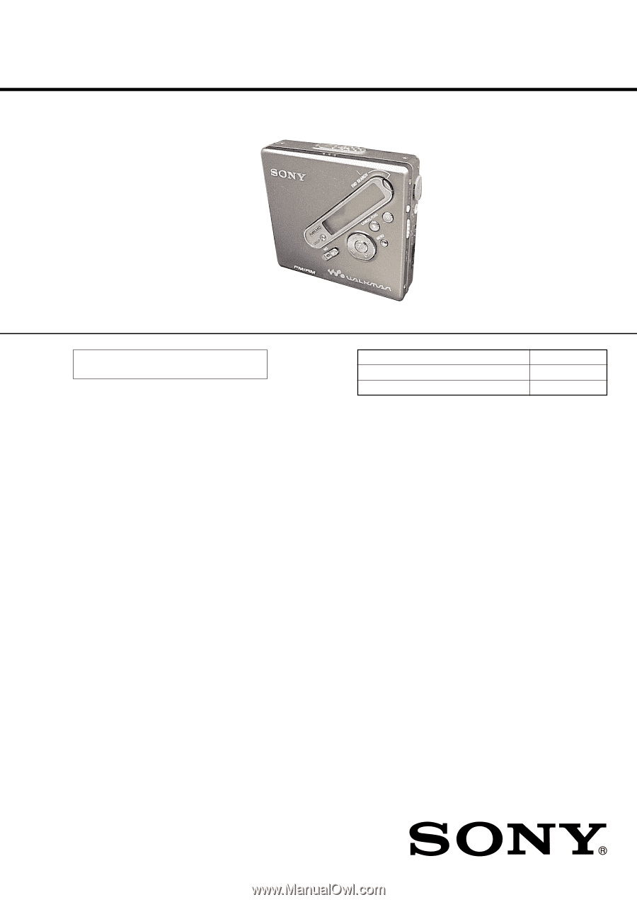
SERVICE MANUAL
PORTABLE MINIDISC RECORDER
US Model
Canadian Model
MZ-NF810CK
AEP Model
UK Model
E Model
Australian Model
Chinese Model
Tourist Model
MZ-NF810
SPECIFICATIONS
MZ-NF810/NF810CK
US and foreign patents licensed from Dolby
Laboratories.
– Continued on next page –
Model Name Using Similar Mechanism
MZ-R410
Mechanism Type
MT-MZN710-177
Optical Pick-up Name
LCX-5R
Ver 1.0
2003. 03
9-877-145-01
Sony Corporation
2003C167800-1
Personal Audio Company
C
2003.03
Published by Sony Engineering Corporation
•
SonicStage, OpenMG and the OpenMG
logo, MagicGate, Memory Stick and the
MagicGate Memory Stick logo,
Memory Stick and the Memory Stick
logo, Net MD and the Net MD logo are
trademarks of Sony Corporation.
•
Microsoft, Windows, Windows NT and
Windows Media are trademarks or
registered trademarks of Microsoft
Corporation in the United States and /or
other countries.
•
IBM and PC/AT are registered
trademarks of International Business
Machines Corporation.
•
Macintosh is a trademark of Apple
Computer, Inc. in the United States and/
or other countries.
•
MMX and Pentium are trademarks or
registered trademarks of Intel
Corporation.
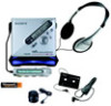
Photo : MZ-NF810
MD recorder
Audio playing system
MiniDisc digital audio system
Laser diode properties
Material: GaAlAs
Wavelength:
λ
= 790 nm
Emission duration: continuous
Laser output: less than 44.6
µ
W
(This output is the value measured at a distance
of 200 mm from the lens surface on the optical
pick-up block with 7 mm aperture.)
Recording and playback time (when
using MDW-80)
Maximum 160 min. in monaural
Maximum 320 min. in LP4 stereo
Revolutions
380 rpm to 2,700 rpm (CLV)
Error correction
ACIRC (Advanced Cross Interleave Reed
Solomon Code)
Sampling frequency
44.1 kHz
Sampling rate converter
Input: 32 kHz/44.1 kHz/48 kHz
Coding
ATRAC (Adaptive TRansform Acoustic
Coding)
ATRAC3 — LP2/LP4