Sony MZ-NF810CK Service Manual - Page 38
Note For Printed Wiring Board And Schematic Diagrams
 |
View all Sony MZ-NF810CK manuals
Add to My Manuals
Save this manual to your list of manuals |
Page 38 highlights
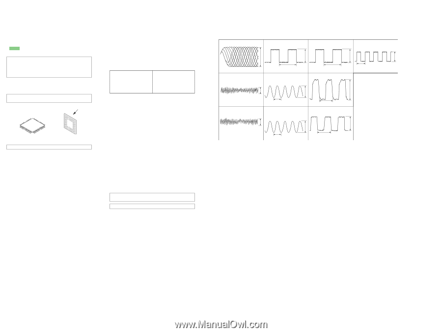
MZ-NF810/NF810CK 6-2. Note For Printed Wiring Board And Schematic Diagrams Note on Printed Wiring Board: • X : parts extracted from the component side. • Y : parts extracted from the conductor side. • : Pattern from the side which enables seeing. (The other layers' patterns are not indicated.) Caution: Pattern face side: (Conductor Side) Parts face side: (Component Side) Parts on the pattern face side seen from the pattern face are indicated. Parts on the parts face side seen from the parts face are indicated. • MAIN board is four-layer printed board. However, the patterns of layers 2 and 3 have not been included in this diagrams. * Replacement of IC501,IC801 on MAIN board requires a special tool. • Lead Layouts surface Lead layout of conventional IC CSP (chip size package) ✩When IC851 is damaged, replace the MAIN board. Note on Schematic Diagram: • All capacitors are in µF unless otherwise noted. pF: µµF 50 WV or less are not indicated except for electrolytics and tantalums. • All resistors are in Ω and 1/4 W or less unless otherwise specified. • % : indicates tolerance. • f : internal component. • C : panel designation. Note: The components identified by mark 0 or dotted line with mark 0 are critical for safety. Replace only with part number specified. Note: Les composants identifiés par une marque 0 sont critiques pour la sécurité. Ne les remplacer que par une pièce portant le numéro spécifié. • A : B+ Line. • Total current is measured with MD installed. • Power voltage is dc 3 V and fed with regulated dc power supply from DC IN 3 V jack (J951). • Voltages and waveforms are dc with respect to ground in playback mode. no mark : PLAYBACK ( ) : REC ∗ : Impossible to measure • Voltages are taken with a VOM (Input impedance 10 MΩ). Voltage variations may be noted due to normal produc- tion tolerances. • Waveforms are taken with a oscilloscope. Voltage variations may be noted due to normal produc- tion tolerances. • Circled numbers refer to waveforms. • Signal path. J : PLAYBACK c : DIGITAL IN F : ANALOG IN f : RECORD N : USB • The voltage and waveform of CSP (chip size package) cannot be measured, because its lead layout is different form that of conventional IC. * Replacement of IC501,IC801 on MAIN board requires a special tool. ✩When IC851 is damaged, replace the MAIN board. • Abbreviation 3CED : Spanish, Swedish, Portuguese and Finnish model 4CED : French, German, Dutch and Italian model • Waveforms 1 4 IC501 9 (RFO)(TP1517) IC601 4 (CLK) 7 IC901 yd (CLK) 0 IC301 q; (LRCK) 2.4Vp-p 2.4Vp-p (REC mode) 500mV/DIV, 200ns/DIV 1.2Vp-p 5.67µs 1V/DIV, 2µs/DIV 2 IC501 rd (TE)(SL501) 5 IC801 2 (OSCO) (at the point of R806) 5.67µs 1V/DIV, 2µs/DIV 8 IC301 9 (MCLK) 22.7µs 1V/DIV, 10µs/DIV 2.4Vp-p 780mVp-p 44.3ns 500mV/DIV, 1ms/DIV 500mV/DIV, 20ns/DIV 2Vp-p 88.6ns 1V/DIV, 40ns/DIV 2.6Vp-p 3 IC501 rs (FE)(SL502) 6 IC801
-
 1
1 -
2
-
3
-
4
-
5
-
6
-
7
-
8
-
9
-
10
-
11
-
12
-
13
-
14
-
15
-
16
-
17
-
18
-
19
-
20
-
21
-
22
-
23
-
24
-
25
-
26
-
27
-
28
-
29
-
30
-
31
-
32
-
 33
33 -
 34
34 -
 35
35 -
 36
36 -
 37
37 -
 38
38 -
 39
39 -
 40
40 -
 41
41 -
 42
42 -
 43
43 -
44
-
45
-
46
-
47
-
48
-
49
-
50
-
51
-
52
-
53
-
54
-
55
-
56
-
57
-
58
-
59
-
60
-
61
-
62
-
63
-
64
-
65
-
66
-
67
-
68
 |
 |