Sony MZ-NF810CK Service Manual - Page 52
Sony MZ-NF810CK Manual
 |
View all Sony MZ-NF810CK manuals
Add to My Manuals
Save this manual to your list of manuals |
Page 52 highlights
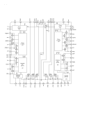
MZ-NF810/NF810CK Pin No. Pin Name I/O Description 111 BATT_CTL O Control signal output for the voltage step up circuit in the external battery case Not used (open) 112 VREC_CTL O VREC voltage control signal output Not used (open) 113 XRST_CHG_IC O Reset signal output to the battery charge control IC 114, 115 PD_S0, 1 O PD IC mode changeover signal output to the optical pick up 116 LINK_MON O Linking area monitor signal output Not used (open) 117 PL_CTL O Plunger control signal output Not used (open) 118 GND_SW O Ground changeover switch control signal output Not used (open) 119, 120 NC O Not used (open) 121 SLD_MON I Sled servo monitor signal input 122 NC O Not used (open) 123 SLEEP O System sleep control signal output to the power control 124 FFCLR O Input latch output for the start switching to the power control 125 CHGI_CTL1 O Charge current limit ON/OFF control signal output at the time of adaptor use 126 CHGI_CTL2 O Charge current limit value changeover control signal output at the time of adaptor use Not used (open) 127 ORANGE_LED O Orange LED ON/OFF control signal output Not used (open) 128 CHG_LED O LED ON/OFF control signal output for CHG (charge display) Not used (open) 129 XTEST I Terminal for the test mode setting (normally open) "L": test mode 130 XRF_RST O Reset control signal output to the RF amplifier "L": reset 131 XEXT_PWR I External power supply (AC adaptor/charging stand) detection signal input 132 XHOLD_SW I HOLD switch input terminal "L": hold ON 133 COUT_MON I Traverse count measurement monitor input 134 CHG_ADSEL O A/D terminal of the battery charge contro IC output selection signal output 135 CHGI_SEL O Charge/discharge changeover control signal output for the current sense amplifier 136 XDC_IN I DC plug detection signal input 137 SPDL_MON I Spindle servo monitor signal input 138 XCS_PWR_IC O Chip select signal output to the power control 139, 140 D_EN1, 2 O Control signal output for the D class headphone amplifier Not used (open) 141 XCS_LCD O Chip select signal output to the liquid crystal display module 142 LCD_STB O Strobe signal output to the liquid crystal display module 143 XRST_MTR_DRV O Reset control signal output to the motor driver "L": reset 144 XCS_NV O Chip select signal output to the nonvolatile memory 145 CHG_PWM O Output voltage control signal output to the battery charge control 146 VREC_PWM O PWM signal output for the Over write head drive power supply voltage control to the REC driver 147 NC O PWM signal output for the laser power supply voltage control to the power control Not used (open) 148 NJM_XMUTE O Muting control signal to the headphone amplifier (NJM type made by JRC) Not used (open) 149 D_VO_PWM O Power supply control signal output for the D class headphone amplifier Not used (open) 150 XCS_REC_DRV O Chip select signal output to the REC driver Not used (open) 151 T_MARK _SW I T MARK (track mark) switch input terminal "L": track mark detection Not used (open) 152 JOG_A I Jog dial pulse input from the switch & liquid crystal display module Not used (open) 153 JOG_B I Jog dial pulse input from the switch & liquid crystal display module Not used (open) 154, 155 NC O Not used (open) 156 SSB_DATA I/O SSB data input/output with the RF amplifier 157 SSB_CLK O SSB clock output to the RF amplifier 158 VBUS_DET I USB power supply voltage detection terminal 159 VB_MON I Voltage monitor input terminal (A/D input) of the UNREG power supply 160 CHG_MON I Decrement of voltage detection and charge/discharge current monitor input from the battery charge control 161 VREF_MON I Reference voltage monitor input (A/D input) from the RF amplifier 162, 163 SET_KEY_1, 2 I Key input (A/D input) from the switch & liquid crystal display module 164 CRADLE_DET I USB cradle or battery case detection signal input Not used (connected to the ground) 165 HIDC_MON I HIGH DC voltage monitor input (A/D input) 52
-
 1
1 -
2
-
3
-
4
-
5
-
6
-
7
-
8
-
9
-
10
-
11
-
12
-
13
-
14
-
15
-
16
-
17
-
18
-
19
-
20
-
21
-
22
-
23
-
24
-
25
-
26
-
27
-
28
-
29
-
30
-
31
-
32
-
33
-
34
-
35
-
36
-
37
-
38
-
39
-
40
-
41
-
42
-
43
-
44
-
45
-
46
-
 47
47 -
 48
48 -
 49
49 -
 50
50 -
 51
51 -
 52
52 -
 53
53 -
 54
54 -
 55
55 -
 56
56 -
 57
57 -
58
-
59
-
60
-
61
-
62
-
63
-
64
-
65
-
66
-
67
-
68
 |
 |
