Asus SP97-XV User Manual - Page 42
Onboard VGA Memory Clock Leave on default setting of Fast
 |
View all Asus SP97-XV manuals
Add to My Manuals
Save this manual to your list of manuals |
Page 42 highlights
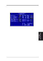
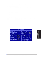
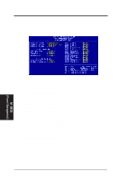
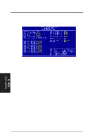
IV. BIOS (Chipset Features) (Chipset Features) IV. BIOS SOFTWARE Linear Mode SRAM Support (Leave on default setting of Disabled) For a slightly better performance on IBM/Cyrix CPUs, this function can be Enabled to switch from Toggle mode SRAM to Linear mode SRAM support. WARNING: Intel CPUs currently only support the Toggle mode so this function should be Disabled when using Intel CPUs. 16-bit ISA Wait State (Leave on default setting of 1 Wait) Timing for 16-bit ISA cards. 16-bit I/O Recovery Time (Leave on default setting of 5 BUSCLK) Timing for 16-bit ISA cards. 8-bit I/O Recovery Time (Leave on default setting of 8 BUSCLK) Timing for 8-bit ISA cards. ISA Bus Clock (Leave on default setting of PCICLK/4) Timing for the ISA bus clock. Video BIOS Cacheable (Leave on default setting of Enabled) This allows the video BIOS to be cached to allow faster execution. Memory Hole at Address (None) This feature reserves memory address space, 15M-16M, 14M-16M, or 12M-16M, to ISA expansion cards that specifically require this setting. This, however, makes the memory from the specified and up unavailable to the system because expansion cards can only access memory up to 16MB. Refresh Cycle Time (187.2 us) This function sets the DRAM refresh rate. A slow refresh cycle time increases the bandwidth available for data transfers. NOTE: Some DRAMs are known to lose data without frequent refreshing so the default is set at 187.2 us. Delayed Transaction (Enabled) The default setting of Enabled frees the PCI Bus during CPU accessing of 8-bit ISA cards, which normally consume about 50-60 PCI clocks without PCI delayed transaction. For PCI bus masters that cannot use the PCI Bus and some ISA cards that are not PCI 2.1 compliant, set this to Disabled. Onboard VGA Memory Size (1MB) This function allows the user to allocate either 1MB, 2MB or 4MB memory for the onboard video controler. Larger memory allows more colors and a higher resoultion to be selected within each operating system. Onboard VGA Memory Clock (Leave on default setting of Fast) This function allows the selection of the video speed. Normal uses 50MHz, Fast uses 60MHz, and Fastest uses 66MHz. If your monitor displays unrecognizable information, you must decrease the speed to match your monitor's frequency rate...Onboard FDC Controller (Enabled) When enabled, this field allows you to connect your floppy disk drives to the onboard floppy drive connector instead of a separate controller card. If you want to use a different controller card, set this field to Disabled. 42 ASUS SP97-XV User's Manual
-
 1
1 -
2
-
3
-
4
-
5
-
6
-
7
-
8
-
9
-
10
-
11
-
12
-
13
-
14
-
15
-
16
-
17
-
18
-
19
-
20
-
21
-
22
-
23
-
24
-
25
-
26
-
27
-
28
-
29
-
30
-
31
-
32
-
33
-
34
-
35
-
36
-
 37
37 -
 38
38 -
 39
39 -
 40
40 -
 41
41 -
 42
42 -
 43
43 -
 44
44 -
 45
45 -
 46
46 -
 47
47 -
48
-
49
-
50
-
51
-
52
-
53
-
54
-
55
-
56
-
57
-
58
-
59
-
60
-
61
-
62
-
63
-
64
-
65
-
66
-
67
-
68
-
69
-
70
-
71
-
72
-
73
-
74
-
75
-
76
-
77
-
78
-
79
-
80
-
81
-
82
-
83
-
84
-
85
-
86
-
87
-
88
-
89
-
90
 |
 |
