Foxconn Z77A-S User manual - Page 40
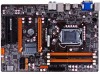
Voltage Configuration, ► Write to Read Delay tWTR
 |
View all Foxconn Z77A-S manuals
Add to My Manuals
Save this manual to your list of manuals |
Page 40 highlights
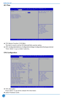
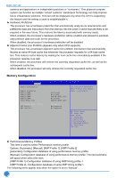
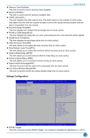
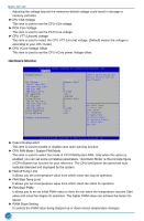
BIOS SETUP ► Memory Clock Multiplier This item is used to set the memory clock multiplier. ► Memory Multiplier This item is used to set the memory multiplier ratio. ► CAS# Latency(tCL) This item dispalys the CAS Latency time. The CAS Latency is the number of clock cycles that elapse from the time the request for data is sent to the actual memory location until the data is transmitted from the module. ► Row Precharge Time(tRP) This item dispalys the DRAM RAS precharge time (in clock cycles). ► RAS# to CAS# Delay(tRCD) This item dispalys the delay time (in clock cycles) between the CAS and RAS strobe signals. ► RAS# Active Time(tRAS) This item dispalys the precharge delay time (in clock cycles). ► Write Recovery Time(tWR) This item allows you to select the write recovery time (in clock cycles). ► Row Refresh Cycle Time(tRFC) This item allows you to select the minimum refresh recovery time (in clock cycles). ► Write to Read Delay (tWTR) This item allows you to set minimum Write-to-read delay (in clock cycles). ► Active to Active Delay (tRRD) This item allows you to set Active to Active Delay (in clock cycles). ► Read CAS# Precharege(tRTP) This item is used to set the read CAS to precharge time (in clock cycles). ►Four Active Window Delay(tFAW) This item is used to set the four active window delay time (in clock cycles). Voltage Configuration Aptio Setup Utility - C opyright (C) 2011 American Megatrends, Inc. OC Plus Voltage Configuration DRAM Voltage CPU VSA Voltage PCH Core Voltage CPU VTT (Uncore) Voltage CPU VCore Voltage offset [Default] [Default] [Default] [Default] [Default] The minimum available for adjustment is 1.307V. The maximum available for adjustment is 2.006V. The default voltage is 1.553V. Adjusting the voltage beyond the memories default voltage could result in damage to memory controller. → ←: Select Screen ↑ ↓: Select Item Enter: Select +/-: Change Opt. F1: General Help F2: Previous Values F3: Optimized Defaults F4: Save & Exit ESC: Exit Version 2.14.1219. Copyright (C) 2011 American Megatrends, Inc. ► DRAM Voltage This item is used to set the DRAM voltage. The maximum available for adjustment is 1.307V. 33
-
 1
1 -
2
-
3
-
4
-
5
-
6
-
7
-
8
-
9
-
10
-
11
-
12
-
13
-
14
-
15
-
16
-
17
-
18
-
19
-
20
-
21
-
22
-
23
-
24
-
25
-
26
-
27
-
28
-
29
-
30
-
31
-
32
-
33
-
34
-
 35
35 -
 36
36 -
 37
37 -
 38
38 -
 39
39 -
 40
40 -
 41
41 -
 42
42 -
 43
43 -
 44
44 -
 45
45 -
46
-
47
-
48
-
49
-
50
-
51
-
52
-
53
-
54
-
55
-
56
-
57
-
58
-
59
-
60
-
61
-
62
-
63
-
64
-
65
-
66
-
67
-
68
-
69
-
70
-
71
-
72
-
73
-
74
-
75
-
76
-
77
-
78
-
79
-
80
-
81
-
82
-
83
-
84
-
85
-
86
-
87
-
88
-
89
-
90
-
91
-
92
-
93
-
94
-
95
-
96
-
97
-
98
-
99
-
100
-
101
-
102
-
103
-
104
-
105
-
106
-
107
-
108
 |
 |