Intel D845HV Product Specification - Page 16
Block Diagram
 |
View all Intel D845HV manuals
Add to My Manuals
Save this manual to your list of manuals |
Page 16 highlights
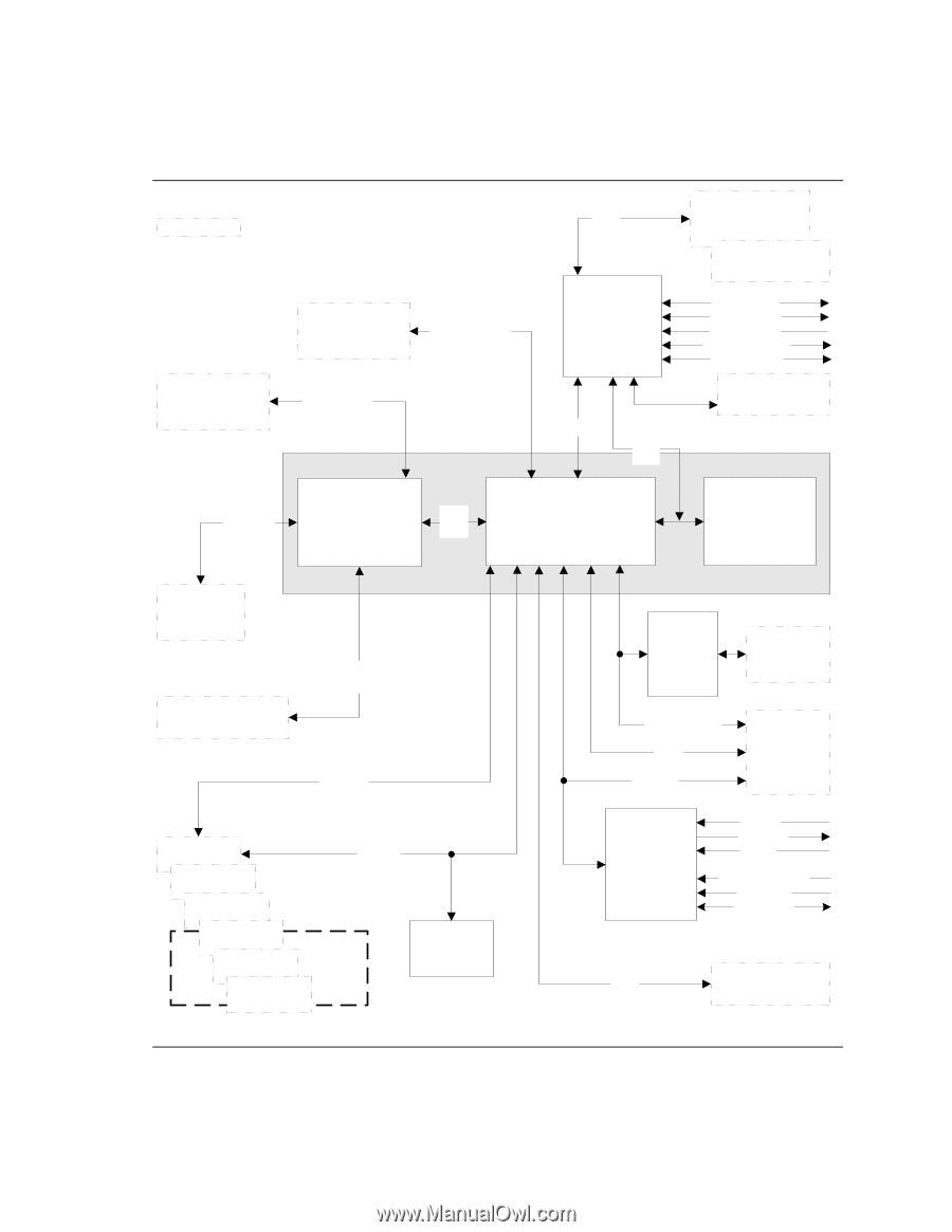
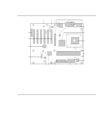
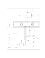
Intel Desktop Board D845HV/D845WN Technical Product Specification 1.2.4 Block Diagram Figure 3 is a block diagram of the major functional areas of the D845HV and D845WN boards. = connector or socket USB Primary/ Secondary IDE UDMA 33 and ATA-66/100 LPC I/O Controller mPGA478 Processor Socket System Bus (400 MHz) AGP Interface 82845 Memory Controller Hub (MCH) USB LPC Bus 845 Chipset AHA Bus 82801BA I/O Controller Hub (ICH2) Back Panel USB Ports (2) Front Panel USB Ports (2) Serial Ports Parallel Port PS/2 Mouse PS/2 Keyboard Infrared Port Diskette Drive Connector 82802AB 4 Mbit Firmware Hub (FWH) 4X AGP Connector (1.5 V only) DIMM Banks (3) SDRAM Bus PCI Bus Physical Layer Interface (optional) CSMA/CD Unit Interface USB AC Link LAN Connector (optional) CNR Connector (optional) PCI Slot 1 SMBus PCI Slot 2 PCI Slot 3 PCI Slot 4 PCI Slot 5 D845WN Only PCI Slot 6 Hardware Monitor (optional) AD1885 Audio Codec (optional) Line In Line Out Mic In Auxiliary Line In CD-ROM Telephony USB Back Panel USB Ports (2) Figure 3. Block Diagram OM12274 16
-
 1
1 -
2
-
3
-
4
-
5
-
6
-
7
-
8
-
9
-
10
-
 11
11 -
 12
12 -
 13
13 -
 14
14 -
 15
15 -
 16
16 -
 17
17 -
 18
18 -
 19
19 -
 20
20 -
 21
21 -
22
-
23
-
24
-
25
-
26
-
27
-
28
-
29
-
30
-
31
-
32
-
33
-
34
-
35
-
36
-
37
-
38
-
39
-
40
-
41
-
42
-
43
-
44
-
45
-
46
-
47
-
48
-
49
-
50
-
51
-
52
-
53
-
54
-
55
-
56
-
57
-
58
-
59
-
60
-
61
-
62
-
63
-
64
-
65
-
66
-
67
-
68
-
69
-
70
-
71
-
72
-
73
-
74
-
75
-
76
-
77
-
78
-
79
-
80
-
81
-
82
-
83
-
84
-
85
-
86
-
87
-
88
-
89
-
90
-
91
-
92
-
93
-
94
-
95
-
96
-
97
-
98
-
99
-
100
-
101
-
102
-
103
-
104
-
105
-
106
-
107
-
108
-
109
-
110
-
111
-
112
-
113
-
114
-
115
-
116
-
117
-
118
-
119
-
120
-
121
-
122
-
123
-
124
-
125
-
126
-
127
-
128
 |
 |