Intel S975XBX2 Product Specification - Page 50
Fixed I/O Map
 |
UPC - 735858186506
View all Intel S975XBX2 manuals
Add to My Manuals
Save this manual to your list of manuals |
Page 50 highlights
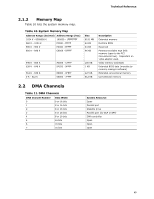
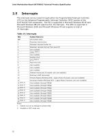
Intel Workstation Board S975XBX2 Technical Product Specification 2.3 Fixed I/O Map Table 12. I/O Map Address (hex) Size Description 0000 - 00FF 256 bytes Used by the Workstation Board S975XBX2. Refer to the ICH7-R/ICH7-DH data sheet for dynamic addressing information. 0170 - 0177 8 bytes Secondary Parallel ATA IDE channel command block 01F0 - 01F7 0228 - 022F (Note 1) 0278 - 027F (Note 1) 02E8 - 02EF (Note 1) 02F8 - 02FF (Note 1) 8 bytes 8 bytes 8 bytes 8 bytes 8 bytes Primary Parallel ATA IDE channel command block LPT3 LPT2 COM4 COM2 0374 - 0377 4 bytes Secondary Parallel ATA IDE channel control block 0377, bits 6:0 7 bits Secondary IDE channel status port 0378 - 037F 8 bytes LPT1 03E8 - 03EF 8 bytes COM3 03F0 - 03F5 6 bytes Diskette channel 03F4 - 03F7 1 byte Primary Parallel ATA IDE channel control block 03F8 - 03FF 8 bytes COM1 04D0 - 04D1 2 bytes Edge/level triggered PIC LPTn + 400 0CF8 - 0CFB (Note 2) 0CF9 (Note 3) 8 bytes 4 bytes 1 byte ECP port, LPTn base address + 400h PCI Conventional bus configuration address register Reset control register 0CFC - 0CFF 4 bytes PCI Conventional bus configuration data register FFA0 - FFA7 8 bytes Primary Parallel ATA IDE bus master registers FFA8 - FFAF 8 bytes Secondary Parallel ATA IDE bus master registers Notes: 1. Default, but can be changed to another address range. 2. Dword access only. 3. Byte access only. NOTE Some additional I/O addresses are not available due to ICH7-R/ICH7-DH address aliasing. The ICH7-R/ICH7-DH data sheet provides more information on address aliasing. For information about Obtaining the ICH7-R/ICH7-DH data sheet Refer to Section 1.2 on page 17 50
-
 1
1 -
2
-
3
-
4
-
5
-
6
-
7
-
8
-
9
-
10
-
11
-
12
-
13
-
14
-
15
-
16
-
17
-
18
-
19
-
20
-
21
-
22
-
23
-
24
-
25
-
26
-
27
-
28
-
29
-
30
-
31
-
32
-
33
-
34
-
35
-
36
-
37
-
38
-
39
-
40
-
41
-
42
-
43
-
44
-
 45
45 -
 46
46 -
 47
47 -
 48
48 -
 49
49 -
 50
50 -
 51
51 -
 52
52 -
 53
53 -
 54
54 -
 55
55 -
56
-
57
-
58
-
59
-
60
-
61
-
62
-
63
-
64
-
65
-
66
-
67
-
68
-
69
-
70
-
71
-
72
-
73
-
74
-
75
-
76
-
77
-
78
-
79
-
80
-
81
-
82
-
83
-
84
-
85
-
86
-
87
-
88
-
89
-
90
-
91
-
92
-
93
-
94
-
95
-
96
-
97
-
98
-
99
-
100
-
101
-
102
 |
 |