Sony HCD-ZUX9 Service Manual - Page 82
Sony HCD-ZUX9 Manual
 |
View all Sony HCD-ZUX9 manuals
Add to My Manuals
Save this manual to your list of manuals |
Page 82 highlights
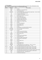
HCD-ZUX9 Pin No. Pin Name I/O [A-TRIG]/ 80 O I/O_EXP RESET 81 A-HALF I 82 FREQ Z-GROOVE O 83 ST-CE O 84 ST-DOUT O 85 ST-CLK O 86 ST-DIN O 87 STBY-LED O 88 GC-RESET O 89 A-SHUT I 90 B-SHUT I 91 B-HALF I 92 ML2252-WR I 93 DEST-IN I 94 THERMAL_VACS I 95 ML2252-BUSY1 I 96 AVSS I [MTK_POWER_MONITOR] 97 I/O CD_BUS0 98 VREF I 99 AVCC - 100 RESET ML2252 I Pin Description Reset signal output to the I/O expander Deck A cassette detection signal input Z-Groove frequency select control signal output "L": Z-Groove "H": Groove PLL chip enable signal output to the tuner unit PLL serial data output to the tuner unit PLL serial data transfer clock signal output to the tuner unit PLL serial data input from the tuner unit LED drive signal output of POWER indicator "H": Green Color "L": Red Color Reset signal output to Display Control IC "L": reset Shut off detection signal input from deck A side reel pulse detector (A/D input) Shut off detection signal input from deck A side reel pulse detector (A/D input) Deck B cassette detection and forward side recording tab detection signal input terminal (A/D input) Data output enable control signal to digital synthesizer ML2252 "L": Data output enable Destination setting terminal Temperature detection signal input from thermistor (A/D input) Channel 1 playback status signal from digital synthesizer ML2252 "H": Playback stop Ground Serial bus data bit 0 input from or output A/D Converter reference voltage input (+3.3V) Power supply (+3.3V) Reset signal output to digital synthesizer ML2252 82
-
 1
1 -
2
-
3
-
4
-
5
-
6
-
7
-
8
-
9
-
10
-
11
-
12
-
13
-
14
-
15
-
16
-
17
-
18
-
19
-
20
-
21
-
22
-
23
-
24
-
25
-
26
-
27
-
28
-
29
-
30
-
31
-
32
-
33
-
34
-
35
-
36
-
37
-
38
-
39
-
40
-
41
-
42
-
43
-
44
-
45
-
46
-
47
-
48
-
49
-
50
-
51
-
52
-
53
-
54
-
55
-
56
-
57
-
58
-
59
-
60
-
61
-
62
-
63
-
64
-
65
-
66
-
67
-
68
-
69
-
70
-
71
-
72
-
73
-
74
-
75
-
76
-
 77
77 -
 78
78 -
 79
79 -
 80
80 -
 81
81 -
 82
82 -
 83
83 -
 84
84 -
 85
85 -
 86
86 -
 87
87 -
88
-
89
-
90
-
91
-
92
-
93
-
94
-
95
-
96
-
97
-
98
-
99
-
100
-
101
-
102
-
103
-
104
-
105
-
106
-
107
-
108
-
109
-
110
-
111
-
112
-
113
-
114
-
115
-
116
-
117
-
118
 |
 |
