Sony HCD-ZUX9 Service Manual - Page 85
Sony HCD-ZUX9 Manual
 |
View all Sony HCD-ZUX9 manuals
Add to My Manuals
Save this manual to your list of manuals |
Page 85 highlights
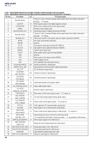
HCD-ZUX9 Pin No. Pin Name I/O 82 P77/X1USB O 83 DVSS - 84 PF0/TXD0 O 85 PF1/RXD0 O PF2/SCLK0/CTS0/ 86 O CLK/TB0OUT0 87 PF3/TXD1/SPDO O 88 PF4/RXD1/SPDI I 89 PF5/SCLK1/CTS1/SPCLK O 90 PN1/SDA0/TA3OUT/SO0 I/O 91 PN2/SCL0/TA2IN/SI0 I/O 92 PN3/HCLK O 93 PN4/HSSO/SDA1 O 94 PN5/HSSI/SCL1 O 95 DVCC3A - 96 PG3 I 97 PG2 I 98, 99 PG1, PG0 I 100 DVSS - Pin Description Not used. (Open) Ground Clear to send signal output to the system controller Serial data signal output Serial data transfer clock signal output Serial data signal output to the system controller Serial data signal input from the system controller Not used in this set. (Open) Two-way EEPROM IIC data bus Not used in this set. Two-way EEPROM IIC clock bus Not used in this set. Bit clock signal output to the CD-MP3 processor Audio data output to the CD-MP3 processor Gate signal output to the CD-MP3 processor Power supply (+3.3 V) Request signal input from the CD-MP3 processor Request signal input from the CD-MP3 processor Function selection signal input Fixed at "H" in this set. Ground 85
-
 1
1 -
2
-
3
-
4
-
5
-
6
-
7
-
8
-
9
-
10
-
11
-
12
-
13
-
14
-
15
-
16
-
17
-
18
-
19
-
20
-
21
-
22
-
23
-
24
-
25
-
26
-
27
-
28
-
29
-
30
-
31
-
32
-
33
-
34
-
35
-
36
-
37
-
38
-
39
-
40
-
41
-
42
-
43
-
44
-
45
-
46
-
47
-
48
-
49
-
50
-
51
-
52
-
53
-
54
-
55
-
56
-
57
-
58
-
59
-
60
-
61
-
62
-
63
-
64
-
65
-
66
-
67
-
68
-
69
-
70
-
71
-
72
-
73
-
74
-
75
-
76
-
77
-
78
-
79
-
 80
80 -
 81
81 -
 82
82 -
 83
83 -
 84
84 -
 85
85 -
 86
86 -
 87
87 -
 88
88 -
 89
89 -
 90
90 -
91
-
92
-
93
-
94
-
95
-
96
-
97
-
98
-
99
-
100
-
101
-
102
-
103
-
104
-
105
-
106
-
107
-
108
-
109
-
110
-
111
-
112
-
113
-
114
-
115
-
116
-
117
-
118
 |
 |
