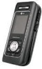
LG M6100 Service Manual
LG M6100 - LG Cell Phone Manual
 |
View all LG M6100 manuals
Add to My Manuals
Save this manual to your list of manuals |
LG M6100 manual content summary:
- LG M6100 | Service Manual - Page 1
Service Manual Model : M6100 Service Manual M6100 Date: February, 2006 / Issue 1.0 - LG M6100 | Service Manual - Page 2
Specification 10 WHITE/FLASH LED LDO 54 3.18 NAND MEMORY 55 3.19 FLIP SWITCH 56 3.20 VIBRATOR 56 3.21 MULTIMEDIA MIC 57 4. TROUBLE SHOOTING 58 4.1 RX Trouble 58 4.2 TX Trouble 64 4.3 Power On Trouble 71 4.4 Charging Trouble 73 4.5 Vibrator Trouble 75 4.6 LCD Trouble 77 4.7 BT Trouble - LG M6100 | Service Manual - Page 3
-4- - LG M6100 | Service Manual - Page 4
steps to maintain telephone service. D. Maintenance Limitations Maintenance limitations on this model must be performed only by the manufacturer or its authorized agent. The user may not make any changes and/or repairs expect as specifically noted in this manual. Therefore, note that unauthorized - LG M6100 | Service Manual - Page 5
the following to the end user. F. Pictures The pictures in this manual are for illustrative purposes only; your actual hardware may look slightly different. G. Interference and Attenuation Phone may interfere with sensitive laboratory equipment, medical equipment, etc.Interference from unsuppressed - LG M6100 | Service Manual - Page 6
INTRODUCTION 1.3 Abbreviations For the purposes of this manual, following abbreviations apply: APC Automatic Power Control Minimum Shift Keying General Purpose Interface Bus Global System for Mobile Communications International Portable User Identity Intermediate Frequency LCD LDO LED - LG M6100 | Service Manual - Page 7
1. INTRODUCTION PAM PCB PGA PLL PSTN RF RLR RMS RTC SAW SIM SLR SRAM PSRAM STMR TA TDD TDMA UART VCO VCTCXO WAP Power Amplifier Module Printed Circuit Board Programmable Gain Amplifier Phase Locked Loop Public Switched Telephone Network Radio Frequency Receiving Loudness Rating Root Mean Square - LG M6100 | Service Manual - Page 8
Display Status Indicator ANT EAR Phone Jack PC Synchronization Speech coding Data and Fax Vibrator Loud Speaker Voice Recoding Microphone Speaker/Receiver Travel Adapter MIDI MP3/AAC Options Feature Li-Poly, 800mAh Battery Size : 34 (W) × 50(H) × 3.8(T) [mm] Battery Weight : TBD Under the minimum - LG M6100 | Service Manual - Page 9
2. PERFORMANCE 2.2 Technical Specification Item Description 1 Frequency Band 2 Phase Error 3 Frequency Error 4 Power Level Specification EGSM TX: 890 + (n-1024) x 0.2 MHz RX: 935 + (n-1024) x 0.2 MHz (n=975~1024) DCS TX: 1710 + (n-512) x 0.2 MHz RX: 1805 + (n-512) x 0.2 MHz (n=512~885) PCS - LG M6100 | Service Manual - Page 10
2. PERFORMANCE Item Description Output RF Spectrum 5 (due to modulation) Output RF Spectrum 6 (due to switching transient) Specification GSM, EGSM Offset from Carrier (kHz). 100 200 250 400 600~ - LG M6100 | Service Manual - Page 11
to switching transient) 7 Spurious Emissions 8 Bit Error Ratio 9 RX Level Report Accuracy 10 SLR 11 Sending Response 12 RLR 13 Receiving Response Specification DCS, PCS Offset from Carrier (kHz). Max. (dBm) 400 -22 600 -24 1,200 -24 1,800 -27 Conduction, Emission Status GSM, EGSM - LG M6100 | Service Manual - Page 12
Tone Distortion System frequency 18 (13 MHz) tolerance 19 32.768KHz tolerance 20 Ringer Volume 21 Charge Current 22 Antenna Display 23 Battery Indicator 24 Low Voltage Warning Specification 13 5 dB > 6 dB dB to ARL (dB) -35 -30 -20 -10 0 7 10 Three stage distortion < 10% Level Ratio (dB) 17.5 22 - LG M6100 | Service Manual - Page 13
2. PERFORMANCE Item Description 25 Forced shut down Voltage 26 Battery Type 27 Travel Charger Specification 3.35 0.03 V 1 Li-Poly Battery Standard Voltage = 3.7 V Battery full charge voltage = 4.2 V Capacity: 800mAh Switching-mode charger Input: 100 ~ 240 V, 50/60 Hz Output: 5.2 V, 800 mA - - LG M6100 | Service Manual - Page 14
power transceiver is a highly integrated device for quad-band Global System for Mobile Communications (GSM), General Packet Radio Service (GPRS), and Enhanced Data for GSM Evolution (EDGE) handsets. The device supports GSM850, EGSM900, DCS1800, and PCS1900 applications. The power transceiver - LG M6100 | Service Manual - Page 15
3. TECHNICAL BRIEF Figure. 3-1 SKY74400 FUNCTIONAL BLOCK DIAGRAM - 16 - - LG M6100 | Service Manual - Page 16
the presence of strong interfering signals. When calibrated correctly, the SKY74400 IP2 meets the GSM AM suppression test requirements in all bands with good margin. A one-time factory calibration procedure produces a set of I/Q compensation coefficients that are programmed in the device to minimize - LG M6100 | Service Manual - Page 17
multiple slot applications such as GPRS. The SKY74400 frequency stepping function with a 3 Hz resolution allows quad band operation in both transmit and receive bands using a fully integrated UHF VCO. The fine synthesizer resolution allows direct compensation or adjustment for reference frequency - LG M6100 | Service Manual - Page 18
high, or low) or the charge pump current can be programmed to a constant value without compensation. Refer to the Skyworks Programming Guide SKY74117 RF Transceiver for Standalone Devices or Embedded MCMs for details. D. Crystal Oscillator A 26 MHz crystal oscillator provides the reference frequency - LG M6100 | Service Manual - Page 19
edge on TXENA initializes the transmit DFC. The output buffers feed the signal to the PAs. Two transmit buffers are provided, one for the low band VCO and the other for the high - LG M6100 | Service Manual - Page 20
Bipolar Transistor (HBT) PA block supports the GSM850 and EGSM900 bands, and the other supports the DCS1800 and PCS1900 bands. Both PA blocks share common The ENABLE input allows initial power-on of PA circuitry to minimize battery drain. (4) Low Drop-Out (LDO) Linear Voltage Regulators The SKY74400 - LG M6100 | Service Manual - Page 21
(Temperature Compensated Crystal Oscillator) which oscillates at a frequency of 13 MHz. It is used within the SKY74400, analog base band chipset (U101, AD6535), digital base band chipset (U103, AD6527B). AFC R507 10K C533 1000p X501 GND VCC 2 4 1 VCONT OUT 3 13MHz 2V75_VVCXO C532 2.2u (1608 - LG M6100 | Service Manual - Page 22
3. TECHNICAL BRIEF ANT_SW3 ANT_SW2 ANT_SW1 C505 27p C506 27p C507 27p FL501 VC3 12 VC2 9 VC1 11 GSM1900_RX GSM1800_RX 6 4 GSM900_RX 2 GND7 16 GND6 15 GND5 14 GND4 GSM18001900_TX 7 5 GND3 GSM900_TX 8 10 GND2 3 1 GND1 LMSP54LA-445TEMP DCS_PCS_TX GSM900_TX 13 ANT Figure 3-4 FEM - LG M6100 | Service Manual - Page 23
Matrix Backlight/ Service Light Flash 16-bit SRAM 8 or 16 bit (optional) DISPLAY (Parallel) serial display Accessory Devices e.g BATTERY SIM Application VCO 13/ 26MHz USC 32KHz AD6535 Audio & Base band Processor JTAG Universal System Connector (USC) Power Management ASDI ASFS ASDO - LG M6100 | Service Manual - Page 24
4K word Program Instruction Cache • Architecture supports Full Rate, Enhanced Support for Pseudo SRAM • Ciphering module for GPRS supporting GAE1 and GAE2 encryption algorithms • Parallel and Serial Display Interface • 8 x 8 Keypad Interface • Four independent programmable backlight plus One Service - LG M6100 | Service Manual - Page 25
through _LCD_CS, LCD_DIM_CTRL, LCD_RESET, LCD_WR, LCD_CS, 2V8_MV, IF_MODE. Signals _LCD_CS LCD_DIM_CTRL LCD_RESET (GPIO 15) _WR 2V8_MV Description MAIN LCD driver chip enable. MAIN LCD driver IC has own CS pin It controls dimming mode of LCD module. This pin resets LCD module. This signal comes - LG M6100 | Service Manual - Page 26
, PA_EN, S_EN, S_DATA, S_CLK, RF_PWR_DWN. Signals Description PA_BAND (GPO 17) PAM Band Select ANT_SW1 (GPO 9) Antenna switch Band Select ANT_SW2 (GPO 11) Antenna switch Band Select ANT_SW3 (GPO 10) Antenna switch Band Select CLKON RF LDO Enable/Disable PA_EN (GPO 16) PAM Enable/Disable - LG M6100 | Service Manual - Page 27
SIM_RST (GPIO_23) Description This pin receives and sends data to SIM card. This model can support only 3.0 volt interface SIM card. Clock 3.25MHz frequency. Reset SIM block Table 3-5. SIM output signal. Interrupt signals are generated by the Auxiliary ADC, audio, and charger modules. - 28 - - LG M6100 | Service Manual - Page 28
Instruction Cache. The micro-controller subsystem supports all the GSM terminal software, including the layer 1, 2 and 3 of the GSM protocol stack, the MMI, and applications software such as data services interfaces to the terminal functions: keyboard, battery supervision, radio and display. Both the - LG M6100 | Service Manual - Page 29
3. TECHNICAL BRIEF 3.5 Analog Main & Power Management Processor (AD6535, U101) Figure 3-8. AD6535 FUNCTIONAL BLOCK DIAGRAM - 30 - - LG M6100 | Service Manual - Page 30
• Light Controllers 4. Audio Section • 8 kHz & 16 kHz Voiceband Codec • 48 kHz Monophonic DAC • Power Amplifiers 5. Power Management section • Voltage Regulators • Battery Charger • Battery Protection 6. Digital Processor section • Control, Baseband, and Audio Serial Ports • Interrupt Logic - 31 - - LG M6100 | Service Manual - Page 31
3. TECHNICAL BRIEF 3.5.1 Baseband Transmit Section 1. The AD6537B Baseband Transmit Section is designed to support GMSK for both single-slot and multi-slot application. 2. The AD6535 includes a digital GMSK modulator which is used for GSM application. The GMSK modulator uses a - LG M6100 | Service Manual - Page 32
Voltage Reference • IDAC: 10 bits • The Auxiliary ADC provides : - Two differential inputs for temperature sensing. - A differential input for the battery charger current sensor CSFS CSDI CSDO AD6535 Control Serial Port AFC DAC Voltage Reference Aux ADC REFTXCM Light Controllers AFCDAC REFBB - LG M6100 | Service Manual - Page 33
3. TECHNICAL BRIEF 3.5.4 Audio Section 1. The AD6535 Audio section supports communications and personal audio applications. 2. The Audio Section provides an audio codec with two digital-to-analog converter, a ring tone volume controller, a microphone interface, and - LG M6100 | Service Manual - Page 34
Figure 3-13. AD6535 POWER MANAGEMENT SECTION 1. Power up sequence logic 1. The AD6535 controls power on sequence 2. Power on sequence - If a battery is inserted, the battery powers the 8 LDOs. - Then if PWRONKEY is detected, the LDOs output turn on. - REFOUT is also enabled - Reset is generated - LG M6100 | Service Manual - Page 35
the microphone interface circuitry (2.5 V, 1 mA) - VVCXO : supplies the voltage controlled crystal oscillator ( 2.75 V, 10 mA) - VBACK : charges the backup battery and supplies the RTC regulator (2.8V, 1.8V) - VAPP : supplies application co-processors such as a touch screen digitizer (3.0V, 1.8V - LG M6100 | Service Manual - Page 36
, and Li-Ion charging control are implemented in hardware. 2. Charging Process - Check charger is inserted or not - If AD6535 detects that Charger is inserted, the CC-CV charging starts. - Exception : When battery voltage is lower than 3.2V, the precharge(low current charge mode) starts firstly - LG M6100 | Service Manual - Page 37
ISL6299 is designed for a single-cell Li-ion or Li-polymer battery charging circuit that accepts both a USB port and a desktop cradle as its power source. Input Auto Selection When both input sources are present, the charger selects only one power source to charge the battery. When the CRDL input is - LG M6100 | Service Manual - Page 38
3. TECHNICAL BRIEF Figure 3-17. BLOCKDIAGRAM Cradle Charge Current The cradle charge current is enabled by the EN pin only, the USBON pin has no control on the cradle charge current. The cradle charge current is programmed with the external resistor connected between the ICDL pin and the GND pin. - LG M6100 | Service Manual - Page 39
input and output voltage comparator, discussed shortly. Both VPOR, VOS have hysteresis, as given in the Electrical Specification table. The charger will not charge the battery if the input voltage does not meet the power-good conditions. Thermal Foldback (Thermaguard™) The thermal foldback function - LG M6100 | Service Manual - Page 40
3.7 CAMERA IC(AIT813,U701) 3. TECHNICAL BRIEF Figure 3-18. AIT813 APPLICATION BLOCKDIAGRAM - 41 - - LG M6100 | Service Manual - Page 41
3. TECHNICAL BRIEF AIT813G 3V3_MULTI_USB VUSB 2V8_MV R705 0 R706 NA C712 1u _LCD_CS C714 33p 2V8_MV R716 47K MULTI_USBMULTI_USB+ _RD _WR _MULTI_RST DATA00 DATA01 DATA02 DATA03 DATA04 DATA05 DATA06 DATA07 DATA08 DATA09 DATA10 DATA11 DATA12 DATA13 DATA14 DATA15 MULTI_BYPASS ADD01 _MULTI_INT - LG M6100 | Service Manual - Page 42
3.8 MIDI IC(YMU787,U708) 3. TECHNICAL BRIEF Figure 3-20. YMU787 BLOCKDIAGRAM - 43 - - LG M6100 | Service Manual - Page 43
3. TECHNICAL BRIEF C733 120p R724 68K TP702 1V8_MV _MIDI_RST C738 0 13MHz 2V8_MV 2V8_VEXT VBAT B4 _RST G5 CLKI D2 BLCK D3 LRCK D1 SDI D6 GPIO0 C5 GPIO1 C1 GPIO2 C4 GPIO3 B1 LED2_GPIO5 C2 LDE1_GPIO4 C3 LED0 B2 MTR FB705 R734 NA C753 0.1u C759 C754 1u 0.1u C760 C761 C762 1u 1u 0.1u - LG M6100 | Service Manual - Page 44
3. TECHNICAL BRIEF CONTROL REGISTER;ROM/SRAM The Control register and ROM/SRAM are accessed from"Instantaneous write register", "Delayed write register", and "Instantaneous read register"in the intermediate register. In the control register, there is a register to control the following synthesizer - LG M6100 | Service Manual - Page 45
and vibrator with a play, and to control. Asynchronous control With a play is also supported. It supports 3 color LED control and it is possible to display 7 colors In maximum. CLOCK GENERATING BLOCK This device supports a clock input ranging from 1.5Mhz to 27Mhz. It is a block to generate a clock - LG M6100 | Service Manual - Page 46
3. TECHNICAL BRIEF 3.9 Keypad Switches and Scanning KEY PAD MAIN CAMERA ROW0, COLO VOL_UP ROW0, COL2 VOL_DOWN ROW0, COL1 (R0,C0) (R0,C1) (R0,C2) CAMERA VOL_DOWN VOL_UP CN301 CN302 3 2 1 4 3 2 1 KEYPAD KEY_ROW_UPPER0 R323 100 R322 100 R321 100 R320 100 R319 100 EVL14K02200 - LG M6100 | Service Manual - Page 47
3. TECHNICAL BRIEF 3.10 Microphone The microphone is placed to the front cover and contacted to main PCB. The audio signal is passed to AIN1P and AININ pins of AD6535. The voltage supply VMIC is output from AD6535, and is a biased voltage for the AIN1P. The AIN1P and AIN1N signals are then A/D - LG M6100 | Service Manual - Page 48
3.12 Headset Interface 3. TECHNICAL BRIEF MIDI_HP_R MIDI_HP_L AUX_OUT_R AUX_OUT_L U203 MAX4684EBC_T V+ B4 C4 NO1 A4 NO2 C1 NC1 A1 NC2 C2 IN1 A2 IN2 C3 COM1 A3 COM2 GND B1 C220 1u HEADSET_PATH_SEL HEADSET_SPK_R HEADSET_SPK_L HEADSET JACK 2V5_VMIC JACK_DETECT L REMOVE H INSERT 1K R201 - LG M6100 | Service Manual - Page 49
3. TECHNICAL BRIEF 3.13 MEMORY(INTEL,U202) 2V8_VMEM MEMORY (INTEL,256MbitFLASH+64Mbit PSRAM) A1 A2 A7 A8 NC1 NC2 NC3 NC4 4.7u 1u _ROM_CS2 _ROM_CS1 C219 0.1u 5 1 VCC 4 3 GND U202 2 TC7SH08FS _ROMCS1 2V8_VMEM 2V8_VMEM 1V8_VCORE ADD01 ADD02 ADD03 ADD04 ADD05 ADD06 ADD07 ADD08 ADD09 - LG M6100 | Service Manual - Page 50
3. TECHNICAL BRIEF 3.14 BLUETOOTH(LBMA-2C67B2,M401) BLUETOOTH VBAT 2V8_VBT R401 330 BT_EN C402 15p C403 2.2u C404 0.1u U401 3 VIN VOUT 4 2 GND BGND STBY NC 6 1 5 BH28FB1WHFV C405 2.2u C406 15p (BT ANT -> TRANSFER TO FETCH ANT) ANT401 FEED NC1 NC2 ABA9030152442 ( 903015 ) - LG M6100 | Service Manual - Page 51
3. TECHNICAL BRIEF 3.15 CAMERA CONNECTOR, CAMERA LDO(CN100,U705) 1V8_CAM 2V6_CAM ENB C_SCK C_SDA C_VS C_HS C_MCLK CN100 1 24 2 23 3 22 4 21 5 20 6 19 7 18 8 17 9 16 10 15 11 14 12 13 C_CD07 C_CD06 C_CD05 C_CD04 C_CD03 C_CD02 C_CD01 C_CD00 C_PCLK C_RST Figure 3-28. - LG M6100 | Service Manual - Page 52
-HLR105 LD102 SSC-TWH104-HLR104 SSC-TWH104-HL R103 47 LD101 KEY_BACKLIGHT R109 12K R110 12K C108 27p 3 2 Q101 2SC5585 1 R111 10 R112 10 KEY_BACKLIGHT_UPPER (WHITE LED) Figure 3-30. MAIN KEY BACKLIGHT VBAT 47 47 47 47 47 47 47 47 C311 1u C312 1u C313 1u C314 1u C315 1u - LG M6100 | Service Manual - Page 53
LED LDO VBAT C713 22u C_FLASH LCD_DIM_CTL R707 R710 0 0 R711 100K R713 100K C707 1u C708 C709 1u 1u WHITE/FLASH LED LDO C3- 1 15 2 12 14 C1+ 11 C2C3+ C2+ C1- 4 VIN 9 17 FB701 FB702 MLED C717 C718 1u 27p C719 C720 27p 27p MLED1 MLED2 Figure 3-32. WHITE/FLASH LED LDO - 54 - - LG M6100 | Service Manual - Page 54
3. TECHNICAL BRIEF 3.18 NAND MEMORY(K9K1G08u0B-J, U702) 1G NAND 2V8_MV R722 10K N_IO(0) N_IO(1) N_IO(2) N_IO(3) N_IO(4) N_IO(5) N_IO(6) N_IO(7) _N_WP _NAND_CS _N_WE _N_RE 2V8_MV N_ALE N_CLE R723 10K R_B R737 0 U707 A1 A2 DU1 B1 DU2 A9 DU3 DU4 A10 DU5 B9 DU6 B10 L1 DU7 L2 DU8 - LG M6100 | Service Manual - Page 55
3. TECHNICAL BRIEF 3.19 FLIP SWITCH (U100) 2V8_VEXT C112 0.1u R120 51K 6 5 VDD OUTPUT 1 2 4 NC2 NC1 7 GND2 3 PGND GND1 U101 A3212EEH-T SLIDE C113 10p Figure 3-34. FLIP SWITCH 3.20 VIBRATOR The vibrator is placed in main board. The vibrator is driven from VIBRATOR from AD6527B. - LG M6100 | Service Manual - Page 56
3. TECHNICAL BRIEF 3.21 MULTIMEDIA MIC(OSF213,MIC201) MULTI_MIC_P MULTI_MIC_N VINNORP VINNORN U201 MAX4684EBC_T V+ B4 C4 NO1 A4 NO2 C1 NC1 A1 NC2 C2 IN1 A2 IN2 C3 COM1 A3 COM2 GND B1 C210 1u MIC_PATH_SEL C206 39p C206 R206 100 39p R208 100 C208 0.1u 2V5_VMIC R202 1K CLOSE TO MIC R203 - LG M6100 | Service Manual - Page 57
4. TROUBLE SHOOTING 4. TROUBLE SHOOTING 4.1 RX Trouble TEST POINT 13Mhz OSCILLATOR SKY74400 FEM Figure 4-1 - 58 - - LG M6100 | Service Manual - Page 58
4. TROUBLE SHOOTING Checking Flow START HP8960 : Test mode 62 CH, 7 level setting (TCH) 62CH, -60dBm setting (BCCH) Spectrum analyzer setting Oscilloscope setting Check VCTCXO Check FEM & Mobile SW Check RX IQ Redownload SW or Do calibration again - 59 - - LG M6100 | Service Manual - Page 59
4. TROUBLE SHOOTING (1) Checking VCTCXO Circuit TEST POINT Checking Flow Check Pin 3. Refer to Graph 4-1(b) 13 MHzO.K? No Check Pin 4. Refer to Graph 4-1(a) 2.75V OK? No Yes VCTCXO Circuit is OK See next Page to check ANT SW & Mobile SW Yes Changing X501 Check U101 CIRCUIT AFC R507 10K - LG M6100 | Service Manual - Page 60
(2) Checking FEM & Mobile SW TEST POINT 4. TROUBLE SHOOTING CIRCUIT ANT_SW3 ANT_SW2 ANT_SW1 Waveform C505 27p C506 27p C507 27p FL501 VC3 12 VC2 9 VC1 11 GSM1900_RX GSM1800_RX 6 4 GSM900_RX 2 GND7 16 GND6 15 - LG M6100 | Service Manual - Page 61
4. TROUBLE SHOOTING Checking Flow For these 2 test case, No Call connection is & FL501.4 Pin6 : ~ -62dBm No (for DCS) & FL501.2 (for PCS) Pin 4,2 : ~ -63dBm Yes FEM & Mobile SW is OK See next Page to check Rx IQ Signal For this RF Level test case, RX Stand alone Mode is needed Changing - LG M6100 | Service Manual - Page 62
4. TROUBLE SHOOTING (4) Checking RX IQ TEST POINT Waveform CIRCUIT 1 VCC3 2 I+_TX_I+ I-_TX_I- 3 Q-_TX_Q- 4 5 Q+_TX_Q+ VCC1 6 C508 22u C509 C512,C513. Check if there is any Major difference Refer to grapa 4-4 Similar? Yes No Replace U501 Redownload software and calibration again - 63 - - LG M6100 | Service Manual - Page 63
4. TROUBLE SHOOTING 4.2 TX Trouble TEST POINT 13Mhz OSCILLATOR SKY74400 FEM Figure 4-2 - 64 - - LG M6100 | Service Manual - Page 64
4. TROUBLE SHOOTING Checking Flow START HP8960 : Test mode 62 CH, 7 level setting (TCH) 62CH, -60dBm setting (BCCH) Spectrum analyzer setting Oscilloscope setting Check VCTCXO Check FEM & Mobile SW Check PAM SIGNAL Check TX IQ Redownload SW or Do calibration again - 65 - - LG M6100 | Service Manual - Page 65
4. TROUBLE SHOOTING (1) Checking VCTCXO Circuit TEST POINT Checking Flow Check Pin 3. Refer to Graph 4-1(b) Check Pin 4. Refer to Graph 4-1(a) Yes 13 MHzO.K? No 2.75V OK? Yes No Check U101 VCTCXO Circuit is OK See next Page to check ANT SW & Mobile SW Changing X501 CIRCUIT AFC R507 10K - LG M6100 | Service Manual - Page 66
(3) Checking Ant SW & Mobile SW TEST POINT 4. TROUBLE SHOOTING ANT 13 CIRCUIT ANT_SW3 ANT_SW2 ANT_SW1 C505 27p C506 27p C507 27p FL501 VC3 12 VC2 9 VC1 11 GSM1900_RX GSM1800_RX 6 4 GSM900_RX 2 GND7 16 GND6 - LG M6100 | Service Manual - Page 67
4. TROUBLE SHOOTING Checking Flow For the test, TX Stand alone Mode is needed. (PL=5 for GSM, PL=0 for DCS) Check C505,C506,C507 Check whether FEM - LG M6100 | Service Manual - Page 68
(4) Checking PAM Control Signal TEST POINT Waveform 4. TROUBLE SHOOTING CIRCUIT R502 0 C520 47p PA_EN TX_RAMP PA_BAND Checking Flow Graph 4-8 Check TX_RAMP and PA_EN Check if there is Any Major Difference or not - Refer to Graph 4 - 8 Similar? Yes Go to Next Step No Download S/W - 69 - - LG M6100 | Service Manual - Page 69
4. TROUBLE SHOOTING (5) Checking TX IQ TEST POINT Waveform CIRCUIT 1 VCC3 2 I+_TX_I+ I-_TX_I- 3 Q-_TX_Q- 4 5 Q+_TX_Q+ VCC1 6 C508 22u C509 33p C510 Flow Check if there is Any Major Difference Refer to Graph 4-9 Similar? Yes No Replace U501 Redownload the Software And calibrate - 70 - - LG M6100 | Service Manual - Page 70
SHOOTING 4.3 Power On Trouble TEST POINT VUSB VCXO VEXT VMIC VABB VMIC VSIM VRTC VMEM VCORE CIRCUIT Figure 4-3 1V8_VCORE 2V8_VMEM 1V8_VRTC 2V85_VSIM 2V75_VABB 2V5_VMIC 2V75_VVCXO VUSB 2V8_VEXT VBAT P1 - LG M6100 | Service Manual - Page 71
VSIM=2.85V (when sim card is inserted) VMIC=2.5V NO Logic level at KEYON of U101 = HIGH YES NO Does it work properly? Re-download software Does it work properly? The power-on procedure is Completed. The problem may NO YES be elsewhere. THE PHONE WILL POWER ON. Replace the main board - 72 - - LG M6100 | Service Manual - Page 72
4.4 Charging Trouble TEST POINT 4. TROUBLE SHOOTING R408 U402 D401 CIRCUIT CUR_MON (ABB AUX2) CHG_EN (GPIO0) VUSBIN VCHARGE Charging IC C407 NA R405 10K R406 0 R410 (1%) R408 R411 10K 39K 10K - LG M6100 | Service Manual - Page 73
NO Voltage across R408 is about 1.2V? YES NO Battery is charged? YES Charging is properly operating Resolder the CN303 Pin 4,5 : VCHARGE Pin12,19,26 : GND The TA is out of order Change the TA Resolder the D401,U402 Replace the D401,U402 The battery may have problems. Change the battery. - 74 - - LG M6100 | Service Manual - Page 74
4.5 Vibrator Trouble TEST POINT 4. TROUBLE SHOOTING Q102 C109 D101 Figure 4-5 Soldering Check CIRCUIT VIBRATOR VBAT R114 R116 1.5K 20 MOTOR R117 7.5K 1 2 3 VBAT Q102 R113 47K R115 220 4 5 6 EMZ2 C110 - LG M6100 | Service Manual - Page 75
4. TROUBLE SHOOTING Checking Flow SETTING : Enter the engineering mode, and set vibrator on at vibration of BB test menu START Is the voltage at pin 6 of - LG M6100 | Service Manual - Page 76
4.6 LCD Trouble TEST POINT 4. TROUBLE SHOOTING Figure 4-5 • Check point - The assembley status of the LCD Module - The Soldering of connector - The FPCB which connects the main board and upper board. - 77 - - LG M6100 | Service Manual - Page 77
4. TROUBLE SHOOTING CIRCUIT DIAGRAM - IF CONNECTOR VSYNCOUT FL601 ICVE21054E250R401FR R601 0 R602 NA 5 G1 10 G2 L_DATA07 L_DATA06 L_DATA05 L_DATA04 C601 C602 C603 C604 NA NA NA - LG M6100 | Service Manual - Page 78
FPCB and boards is OK? Yes CN601& CN102 is soldered well? Yes Paths of LCD control signals are OK? Yes No Refer to Power On Trouble No Reconnect FPCB No Re-solder the CN601 & CN102 No Re-solder the EMI filter FPCB is OK? No Replace the FPCB Yes Connection between - LG M6100 | Service Manual - Page 79
SHOOTING 4.7 BT Trouble TEST POINT BT_EN _BT_RST DUBUG_TX Figure 4-7 DUBUG_RX CIRCUIT DIAGRAM BLUETOOTH VBAT 2V8_VBT R401 330 BT_EN C402 15p C403 2.2u C404 0.1u U401 3 VIN VOUT GND - LG M6100 | Service Manual - Page 80
4. TROUBLE SHOOTING Checking Flow Is BT_RST signal shape similar to Fig.1 during Powering on Bluetooth Yes 2V8_VBT at C405=2.8V Bluetooth Power off Is DEBUG_TX signal - LG M6100 | Service Manual - Page 81
4. TROUBLE SHOOTING Graph 4-10(a) BLUE-RST Graph 4-10(b) DEBUG_TX,RX Graph 4-10(c) PCM_SYNCS,TX,RX,USC0 - 82 - - LG M6100 | Service Manual - Page 82
4.8 Speaker Trouble TEST POINT C743 C744 4. TROUBLE SHOOTING CIRCUIT DIAGRAM B8 SPOUT2L B7 SPOUT1L H8 SPOUT2R J8 SPOUT1R E8 TXOUT D7 EXTOUT C743 C744 47p 47p C742 NA R732 NA R731 0 R733 0 Close to SPEAKER SPK_N SPK_P - 83 - - LG M6100 | Service Manual - Page 83
4. TROUBLE SHOOTING Checking Flow START Check the state of contact of dual speaker Yes No Reassemble speaker C743,C744 are Well-soldered? No Re-solder C743,C744 Yes Check U708 works properly No Re-solder U708 Yes Speaker Works properly? Yes Speaker working! No Change main board - 84 - - LG M6100 | Service Manual - Page 84
4. TROUBLE SHOOTING 4.9 SIM Card Interface Trouble TEST POINT CIRCUIT DIAGRAM Figure 4-9 SIM CONNECTOR 2V85_VSIM 2V85_VSIM R362 0 SIM_DATA R361 20K C321 NA J301 4 5 GND1 VCC 1 2 6 VPP IO RST CLK 3 10 9 GND5 GND2 7 8 - LG M6100 | Service Manual - Page 85
4. TROUBLE SHOOTING Checking Flow START Does the SIM cards NO Change the SIM Card. Our phone supports 2.85V ? supports only 3V SIM card. YES Voltage at pin1 of NO J301 is 2.85V? YES Voltage at VSIM of U101 Is 2.85V? NO YES Replace J301 - LG M6100 | Service Manual - Page 86
4.10 Earphone Trouble TEST POINT 4. TROUBLE SHOOTING C209 C211 Figure 4-10 U203 CIRCUIT DIAGRAM 2V5_VMIC 1K R201 HEADSET_MICP HEADSET_MICN R205 100 R207 100 C205 0.1u R204 2.2K C202 C204 10u 39p - LG M6100 | Service Manual - Page 87
4. TROUBLE SHOOTING Checking Flow START Resolder CN201 Does the audio profile of the phone change to the earphone mode? YES NO Level at NO JACK_DETECT signal is low YES Replace CN201 Set the audio part of the test Equipment - LG M6100 | Service Manual - Page 88
Trouble TEST C319 1 2SC5585 27p R359 10 R360 10 LEBB-S14H X 8EA KEY_BACKLIGHT (WHITE LED) Main PCB START Is the voltage level VBAT 3.6-4.2V? Yes Are Charge battery No Check the soldering of each R or replace LEDs not working. No Check the condition of Q302. If problem, Change Q301 - 89 - LG M6100 | Service Manual - Page 89
4. TROUBLE SHOOTING TEST POINT CIRCUIT VBAT 47 47 47 47 C101 1u C102 1u C103 1u Are all LEDs LD100~LD105 working? Yes Q100 is working? Yes BACKLIGHT WILL WORK PROPERLY. No Charge battery No Check the soldering of each R or replace LEDs not working. No Check the condition of Q100. If - LG M6100 | Service Manual - Page 90
SHOOTING 4.12 Receiver Trouble TEST POINT R114 R116 Figure 4-13 CIRCUIT DIAGRAM AOUT1P J15 K15 AOUT1N AOUT2P1 R11 AOUT2P2 T11 T9 AOUT2N1 AOUT2N2 R9 AOUT3L J16 K16 AOUT3R GPI - LG M6100 | Service Manual - Page 91
TROUBLE SHOOTING Checking Flow SETTING : After initialize Agilent 8960, Test EGSM, DCS, PCS mode Set the property of audio as PRBS or continuous wave. Set the receiving volume of mobile as Check the contact state of dual mode speaker. Yes The dual mode speaker will work properly. No Replace the - LG M6100 | Service Manual - Page 92
SHOOTING 4.13 Microphone Trouble TEST POINT U201 R206 R202 R203 CIRCUIT DIAGRAM R208 C208 Figure 4-14 1V8_VCORE 2V8_VMEM 1V8_VRTC 2V85_VSIM 2V75_VABB 2V5_VMIC 2V75_VVCXO VUSB 2V8_VEXT VBAT P1 VCORE1 VCORE2 - LG M6100 | Service Manual - Page 93
4. TROUBLE SHOOTING Checking Flow SETTING : After initialize Agilent 8960, Test EGSM, DCS, PCS mode START No Voltage across C120 is about 2.5V? MIC Bias Voltage Yes - LG M6100 | Service Manual - Page 94
4.14 RTC Trouble TEST POINT 4. TROUBLE SHOOTING Figure 4-15 CIRCUIT DIAGRAM X101 NA 3 C130 4 (FROM TCXO) CLKON C131 R108 2 1 10M PWRON MC-146_7pF 32.768KHz C132 NA CHG_EN CHG_STAT BT_EN 1000p - LG M6100 | Service Manual - Page 95
4. TROUBLE SHOOTING Checking Flow START Is the voltage level of BAT101 > 1.2V ? NO Charge or change BAT101. YES Check the voltage at NO 1,4 of X101 YES Change main board Resolder R108 or Replace X101 - 96 - - LG M6100 | Service Manual - Page 96
4.15 Slide on/off Trouble Test Points 4. TROUBLE SHOOTING Circuit Diagram Figure 4-16 SLIDE 2V8_VEXT C112 0.1u R120 51K 6 5 VDD OUTPUT 1 2 4 NC2 NC1 7 GND2 3 PGND GND1 U101 A3212EEH-T SLIDE C113 10p - 97 - - LG M6100 | Service Manual - Page 97
4. TROUBLE SHOOTING Checking Flow START Check the magnet No in upper side Place the magnet Yes Voltage at Pin 6 of U101 = 2.8V =0V? Yes Does it work properly ? Yes FOLDER WILL WORK PROPERLY. No Resolder R202 & U200 No Replace U200 No Re-download software or Change the main board. - 98 - - LG M6100 | Service Manual - Page 98
4. TROUBLE SHOOTING 4.16 Camera and Flash Trouble U705 CN802 U704 Camera Module Figure 4-17 - 99 - - LG M6100 | Service Manual - Page 99
4. TROUBLE SHOOTING Circuit Diagram 2V8_MV R716 47K MULTI_BYPASS ADD01 _MULTI_INT _WAIT 13MHz C725 1000p DATA00 DATA01 DATA02 DATA03 DATA04 DATA05 DATA06 DATA07 DATA08 DATA09 DATA10 DATA11 - LG M6100 | Service Manual - Page 100
Flow START Does LCD work properly? No Go to the LCD Trouble Yes Set the Camera button ON Yes No Check power 1.8V Yes No Check the 17MHz waveform? Check power U705 No 1V8_CAM No Check U704 - LG M6100 | Service Manual - Page 101
5. DOWNLOAD AND CALIBRATION 5. DOWNLOAD AND CALIBRATION 5.1 Download A. Download Setup Figure 5-1 describes Download setup UART (If you have battery, no TA is needed) Figure 5-1. Download Setup - 102 - - LG M6100 | Service Manual - Page 102
5. DOWNLOAD AND CALIBRATION B. Download Procedure 1. Create a new folder on C: Drive as below after downloading GSMULTI program on GCSC. 2. Execute by double- click 1. Execute by double- click 2. Execution and Configuration Setting 1. Setting -> Configuration - 103 - 2. Select *.dll file - LG M6100 | Service Manual - Page 103
5. DOWNLOAD AND CALIBRATION 3. Click 'Start' button and then connect the phone and the cable. " START " BTN Click - 104 - - LG M6100 | Service Manual - Page 104
port End Com port USE no3.cPhreecsks Start and Wait Model DLL File select (C:\GSMULTI\Model) Phone Software select (mot,m0 file) Donít changed Frame count select ìHermesîselect in case M6100 External boot select (Only TI Model ) (External boot : G7000, G7030 ) After setting completed "OK" BTN - LG M6100 | Service Manual - Page 105
GPIO interface card Calibration & Final test software Test SIM Card PC (for Software Installation) Type / Model HP-8960 HP-66311B HP-GPIB Pentium II class above 300MHz B. Equipment Setup Brand Agilent LG LG Agilent Agilent LG GSM Test Set(8960) GPIB Cable MMoboibleileSSwwitcithchCCabalbele - LG M6100 | Service Manual - Page 106
2 Switch 3 Switch 4 Name ADI-REMOTE TI-REMOTE VBAT PS Description In ON state, phone is awaked. It is used ADI chipset. In ON state, phone is awaked. It is used TI chipset. Power is provided for phone from battery Power is provided for phone from Power supply Table 5-3 Jig DIP Switch - 107 - - LG M6100 | Service Manual - Page 107
Number LED 1 LED 2 LED 3 LED 4 Name Power TA UART MON Description Power is provided for Test Jig Indicate charging state of the phone battery Indicate data transfer state through the UART port Indicate data transfer state through the MON port Table 5-4 LED Description 1. Connect as Fig 6-2(RS232 - LG M6100 | Service Manual - Page 108
6. BLOCK DIAGRAM X1(M6100) Block Diagram(05.08.20) - 109 - LCD_DIMM _CTRL C_FLASH DEBUG_TX /DEBUG_RS USC(0:6) /L_RD/L_A0 VMLED(1:4) LCD SUB CAM_FLASH MULTI_MIC_P/MULTI_MIC_N KEYBACKLIGHT EL_OUT EL DRIVER MIC_PAHT_SEL LDO CAM_AF_EN CAM_PWR_EN HS/VS/SCK/SDA/ MULTI_CLK_OUT CMA_RST C_CD(0:7) - LG M6100 | Service Manual - Page 109
- 110 - - LG M6100 | Service Manual - Page 110
8 9 10 1V8_VCORE 2V8_VMEM 2V8_VEXT 2V8_VMEM 2V85_VSIM VUSB 1V8_VRTC Speaker Phone Pwr D101 RPWRON R106 100K 2 3 1 KDR331V ONNOFF PWRON 02 2005 Approved Sign & Name MODEL M6100 (X1) Sheet/Sheets 1 / 7 DRAWING Hermes 6527B / TyphoonB 6535 NAME LG Electronics Inc. DRAWING NO. REV.1.1 - LG M6100 | Service Manual - Page 111
C221 1u SPK_RCV_SEL SPK_RCV_P D SPK_RCV_N SPK_RCV_SEL L RECEIVER H SPEAKER Notice No. Date Name Section Designer Checked Approved Date 09/02 2005 Sign & Name MODEL DRAWING NAME LG Electronics Inc. DRAWING NO. M6100(X1) Sheet/Sheets 2 / 7 MEMORY/EARJACK/MIC REV - LG M6100 | Service Manual - Page 112
KEY_BACKLIGHT R357 12K 2 R358 C319 1 2SC5585 12K 27p R359 10 R360 10 KEY_BACKLIGHT (WHITE LED) R361 J301 20K 4 5 GND1 VCC 1 2 R362 0 SIM_DATA 6 VPP IO Approved Sign & Name MODEL DRAWING NAME LG Electronics Inc. DRAWING NO. M6100(X1) Sheet/Sheets 3 / 7 KEY/SIM/IO/VIB REV - LG M6100 | Service Manual - Page 113
PCM_TX PCM_RX PCM_SYNC8 USC0 B1 GND 10K D Iss. 5 Notice No. Date Name Section Designer Checked Approved Date 09/02 2005 Sign & Name MODEL DRAWING NAME LG Electronics Inc. DRAWING NO. M6100(X1) Sheet/Sheets 4 / 7 CHARGING/BT/UART REV - LG M6100 | Service Manual - Page 114
C529 NA NA D 13MHz (TO CAM) 13MHz (TO DBB) 13MHz (TO MIDI) Section Designer Checked Approved Date 09/02 2005 Sign & Name MODEL DRAWING NAME M6100(X1) Sheet/Sheets 5 / 7 RF(SKYWORKS CHIPSET) Iss. Notice No. Date Name - LG M6100 | Service Manual - Page 115
NA C644 NA C_HS C_MCLK C_PCLK C_RST D Iss. 5 Notice No. Date Name Section Designer Checked Approved Date 09/02 2005 Sign & Name MODEL DRAWING NAME LG Electronics Inc. DRAWING NO. M6100(X1) Sheet/Sheets 6 / 7 I/F CONNECTOR REV - LG M6100 | Service Manual - Page 116
3 VIN VOUT 4 150mA C711 1u (1005) A C707 1u C708 C709 1u 1u WHITE/FLASH LED LDO VBAT C3- 1 2 15 12 14 C1+ 11 C2C3+ C2+ C1 2005 Approved Sign & Name MODEL DRAWING NAME M6100(X1) Sheet/Sheets 7/7 CAMERA IC / MIDI / MEMORY H Date Name LG Electronics Inc. DRAWING NO. REV.1.1 2 - LG M6100 | Service Manual - Page 117
2SC5585 1 27p R110 12K C108 R111 10 R112 10 D KEY_BACKLIGHT_UPPER (WHITE LED) E AXK7L20227G 2V8_VEXT VBAT CN101 G1 G2 1 20 KEY_ROW_UPPER0 2 & Name MODEL DRAWING NAME Iss. Notice No. Date Name 8 9 8 LG Electronics Inc. 10 DRAWING NO. Sheet/Sheets X1 1/1 UPPER / KEY PCB - LG M6100 | Service Manual - Page 118
47p C101 27p C102 47p VA100 EVLC14S02050 VA101 EVLC14S02050 OUT100 OUT101 E WHITE/FLASH LED R103 180 FLASH 4 R104 180 1 3 R105 Sign & Name MODEL M6100(X1) Sheet/Sheets 1/1 Checked Approved DRAWING NAME UPPER / KEY PCB H Iss. Notice No. Date Name LG Electronics Inc. DRAWING NO - LG M6100 | Service Manual - Page 119
8. PCB LAYOUT - 120 - - LG M6100 | Service Manual - Page 120
8. PCB LAYOUT - 121 - - LG M6100 | Service Manual - Page 121
8. PCB LAYOUT - 122 - - LG M6100 | Service Manual - Page 122
8. PCB LAYOUT - 123 - - LG M6100 | Service Manual - Page 123
- 124 - - LG M6100 | Service Manual - Page 124
About Engineering Mode Engineering mode is designed to allow a service man/engineer to view and test the basic functions provided by Reset S/W Version LCD CAMERA LED BACKLIGHT BUZZER VIBRATOR ADC BATTERY AUDIO DAI BLUETOOTH SAR Test All Auto Test Backlight Buzzer Vibrator LCD Key pad MicSpkTest - LG M6100 | Service Manual - Page 125
MODE 9.1 BB Test [MENU 1] 9.1.1 LCD 1) COLOUR : WHITE, RED, GREEN, BLUE, BLACK 9.1.2 CAMERA This menu is to controls brightness of Backlight. When entering into the menu, the present backlight-value in the phone is displayed. Use Left/Right key to adjust the level of brightness. The value of - LG M6100 | Service Manual - Page 126
Voltage Battery ADC 2) AUX ADC : Auxiliary ADC 3) TEMPER ADC : Temperature ADC 9.1.8 BATTERY 1) Bat Cal : This displays the value of Battery Calibration. over, it returns to default value after switching off and on the phone. 1) VbControl1 : VbControl1 bit Register Value Setting 2) VbControl2 : - LG M6100 | Service Manual - Page 127
9. ENGINEERING MODE 9.2 RF Test [MENU 2] 9.2.1 SAR test This menu is to test the Specific Absorption Rate. 1) SAR test on : Phone continuously process TX only. Call-setup equipment is not required. 2) SAR test off : TX process off 9.3 MF mode [MENU 3] This manufacturing mode is designed to do the - LG M6100 | Service Manual - Page 128
should NOT progress this menu, otherwise some of valuable data such as Setting value, RF Calibration data, etc. cannot be restored again. 9.7 S/W version This displays software version stored in the phone. - 129 - - LG M6100 | Service Manual - Page 129
manual explains how to examine the status of RX and TX of the model. A. Tx Test TX test - this is to see if the transmitter of the phones is input the values. C. Rx 1. Selecting Channel - Select one of GSM or DCS Band and input appropriate channel. 2. Gain Control Index (0~ 26) and RSSI level - See - LG M6100 | Service Manual - Page 130
10. STAND ALONE TEST 10.3 Means of Test a. Select a COM port b. Set the values in Tx or Rx c. Select band and channel d. After setting them all above, press connect button. e. Press the start button Figure 10-1. HW test program - 131 - - LG M6100 | Service Manual - Page 131
10. STAND ALONE TEST Figure 10-2. HW test setting Figure 10-3. Ramping profile - 132 - - LG M6100 | Service Manual - Page 132
the PC side Calibration tool that perform Tx ,Rx and Battery Calibration with Agilent 8960(GSM call setting instrument) and Tektronix PS2521G installed with Microsoft Windows 2000/XP - Auto Calibration program (Hot_kimchi) - GSM Phone - LGE PIF JIG, Serial Cable, Data Cable - Agilent 8960 or CMU200 - LG M6100 | Service Manual - Page 133
11. AUTO CALIBRATION -. To set up Data route, info_Db.TXT should be edited. -. The names in the cycle should be same. 11.4 How to do calibration 1. Run file name is "Hot_kinchiD.exe" 1 - 134 - - LG M6100 | Service Manual - Page 134
2. Choose the Model name of mobile phone. 3. Push the "APPLY" button. 4. Push the "CALIBRATION START" button. 11. AUTO CALIBRATION - 135 - - LG M6100 | Service Manual - Page 135
11. AUTO CALIBRATION 5. Push the "START" button. Cable Loss : Enter the RF cable loss GSM and DCS 6. Phone test finish is shown in below screen. - 136 - - LG M6100 | Service Manual - Page 136
12. EXPLODED VIEW & REPLACEMENT PART LIST 12.1 EXPLODED VIEW 10 4 6 8 21 13 14 15 17 12 23 24 25 26 29 31 32 34 1 2 3 5 7 9 37 36 35 27 33 30 18 11 16 19 20 22 41 43 40 38 39 46 28 50 49 44 42 45 48 47 - 137 - - LG M6100 | Service Manual - Page 137
- 138 - - LG M6100 | Service Manual - Page 138
MAGNET,SWITCH 5 MSHY00 SUPPORT 5 MTAA00 TAPE,DECO 5 MTAB00 TAPE,PROTECTION 5 MTAZ00 TAPE 5 MTAZ01 TAPE 4 ACGR00 COVER ASSY, SLIDE(LOWER) 5 MCJV00 COVER,SLIDE(LOWER) 5 MDAD00 DECO,CAMERA Part Number Specification TGLL0002601 AAAY0138001 M6100 EUASV APEY0243601 ABGA0005601 - LG M6100 | Service Manual - Page 139
SUPPORT 5 MTAA00 TAPE,DECO 5 MTAB00 TAPE,PROTECTION 5 MTAB01 TAPE,PROTECTION 5 MTAD00 TAPE,WINDOW 5 MWAE00 WINDOW,CAMERA Part Number Specification MTAA0099101 M6100 RECEIVER Silver 10 Silver 6 Silver 9 Black 4 Black 12 Gold Black White 8 Black 7 White 15 Gold - LG M6100 | Service Manual - Page 140
MOBILE SWITCH 3 MLAK00 LABEL,MODEL 5 ADCA00 DOME ASSY,METAL 5 MLAB00 LABEL,A/S Part Number Specification mechanical) MPBF0013501 MRAY0003601 M6100 PLASTIC HINGE MTAB0090501 MTAZ0106101 Black Silver White Gold Gold Blue Without Color Silver Without Color Silver Remark 2 30 1 5 11 Silver 40 - LG M6100 | Service Manual - Page 141
5 SAEB00 PCB ASSY, KEYPAD,INSERT 6 SBCL00 BATTERY,CELL,LITHIUM 6 SJMY00 VIBRATOR,MOTOR 5 SAEE00 PCB ASSY,KEYPAD,SMT 6 SAEC00 PCB ASSY,KEYPAD,SMT BOTTOM 7 C107 CAP,CERAMIC,CHIP 7 C108 CAP,CERAMIC,CHIP Part Number Specification SNGF0011901 3.0:1 ,-2 dBd, ,3.0:1,-2.0 GSM,DCS,PCS - LG M6100 | Service Manual - Page 142
7 VA102 VARISTOR 7 VA103 VARISTOR 7 VA104 VARISTOR 6 SAED00 PCB ASSY,KEYPAD,SMT TOP 7 C101 CAP,CERAMIC,CHIP 7 C102 CAP,CERAMIC,CHIP Part Number Specification ECCH0006201 4.7 uF,6.3V ,K ,X5R ,TC ,1608 ,R/TP ECCH0000115 22 pF,50V,J,NP0,TC,1005,R/TP ECCH0000115 22 pF,50V,J,NP0,TC,1005 - LG M6100 | Service Manual - Page 143
,CHIP Part Number Specification ECCH0004904 1 uF,6. WHITE ,1608 ,R/TP ,PB-FREE(ZENER) EDLH0011901 WHITE ,1608 ,R/TP ,PB-FREE(ZENER) EDLH0011901 WHITE ,1608 ,R/TP ,PB-FREE(ZENER) EDLH0011901 WHITE ,1608 ,R/TP ,PB-FREE(ZENER) EDLH0011901 WHITE ,1608 ,R/TP ,PB-FREE(ZENER) EDLH0011901 WHITE - LG M6100 | Service Manual - Page 144
,CHIP 6 C138 CAP,CERAMIC,CHIP 6 C139 CAP,CERAMIC,CHIP 6 C140 CAP,CERAMIC,CHIP 6 C141 CAP,CERAMIC,CHIP 6 C142 CAP,CERAMIC,CHIP Part Number Specification ECCH0004903 1 uF,6.3V ,Z ,Y5V ,TC ,1005 ,R/TP ECCH0000163 47 nF,10V,K,X5R,HD,1005,R/TP ECCH0000163 47 nF,10V,K,X5R,HD,1005,R/TP - LG M6100 | Service Manual - Page 145
12. EXPLODED VIEW & REPLACEMENT PART LIST Level 6 Location No. Description C143 CAP,CERAMIC,CHIP Part Number Specification ECCH0000120 39 pF,50V,J,NP0,TC,1005,R/TP 6 C144 CAP,CERAMIC,CHIP ECCH0000120 39 pF,50V,J,NP0,TC,1005,R/TP 6 C145 CAP,CERAMIC,CHIP ECCH0000120 - LG M6100 | Service Manual - Page 146
12. EXPLODED VIEW & REPLACEMENT PART LIST Level 6 Location No. Description C301 CAP,CERAMIC,CHIP Part Number Specification ECCH0004904 1 uF,6.3V ,K ,X5R ,TC ,1005 ,R/TP 6 C302 CAP,TANTAL,CHIP,MAKER ECTZ0004201 22 uF,6.3V ,M ,STD ,2012 ,R/TP 6 C303 CAP,TANTAL,CHIP,MAKER ECTZ0004201 - LG M6100 | Service Manual - Page 147
,CHIP 6 C718 CAP,CERAMIC,CHIP 6 C719 CAP,CERAMIC,CHIP 6 C720 CAP,CERAMIC,CHIP 6 C725 CAP,CERAMIC,CHIP 6 C763 CAP,CERAMIC,CHIP Part Number Specification ECCH0000186 33 pF,50V ,J ,NP0 ,TC ,1005 ,R/TP ECCH0000182 0.1 uF,10V ,K ,X5R ,HD ,1005 ,R/TP ECCH0000120 39 pF,50V,J,NP0,TC,1005,R/TP - LG M6100 | Service Manual - Page 148
R201 RES,CHIP 6 R202 RES,CHIP 6 R203 RES,CHIP 6 R204 RES,CHIP 6 R205 RES,CHIP 6 R206 RES,CHIP 6 R207 RES,CHIP Part Number Specification ENJE0003602 12 ,12 PIN,MMIC CONN.12P ENRY0005301 3 PIN,0.5 mm,ETC , ,1.48Offset EDSY0017301 VSM ,15 V,100 mA,R/TP ,PB-FREE EDSY0012101 US-FLAT ,30 - LG M6100 | Service Manual - Page 149
RES,CHIP 6 R333 RES,CHIP 6 R334 RES,CHIP 6 R335 RES,CHIP 6 R336 RES,CHIP 6 R341 RES,CHIP 6 R352 RES,CHIP Part Number Specification ERHY0000220 100 ohm,1/16W,J,1005,R/TP ERHY0000247 2.2K ohm,1/16W,J,1005,R/TP ERHY0000202 4.7 ohm,1/16W,J,1005,R/TP ERHY0000247 2.2K ohm,1/16W,J,1005 - LG M6100 | Service Manual - Page 150
6 R507 RES,CHIP 6 R702 RES,CHIP 6 R705 RES,CHIP 6 R707 RES,CHIP 6 R710 RES,CHIP 6 R711 RES,CHIP Part Number Specification ERHY0000201 0 ohm,1/16W,J,1005,R/TP ERHY0000201 0 ohm,1/16W,J,1005,R/TP ERHY0000201 0 ohm,1/16W,J,1005,R/TP ERHY0000201 0 ohm,1/16W,J,1005,R/TP ERHY0000265 20K - LG M6100 | Service Manual - Page 151
TVS 6 VA204 DIODE,TVS 6 VA205 DIODE,TVS Part Number Specification ERHY0000280 100K ohm,1/16W,J,1005,R/TP ERHY0000261 10K ohm,1/16W,J,1005 Charger IC, I Max 1A, Wall Adaptor/USB Charger SON5-P-0.35(fSV) ,5 PIN,R/TP ,2-INPUT AND GATE, Pb EUSY0227901 Free EUSY0163901 uCSP ,10 PIN,R/TP ,Dual - LG M6100 | Service Manual - Page 152
6 VA210 DIODE,TVS 6 VA211 DIODE,TVS 6 VA212 DIODE,TVS 6 VA306 VARISTOR 6 VA307 VARISTOR 6 VA308 VARISTOR 6 VA309 VARISTOR Part Number Specification EDTY0008501 TFSC ,5 V,50 W,R/TP ,small size EDTY0008501 TFSC ,5 V,50 W,R/TP ,small size EDTY0008501 TFSC ,5 V,50 W,R/TP ,small size - LG M6100 | Service Manual - Page 153
12. EXPLODED VIEW & REPLACEMENT PART LIST Level 6 Location No. Description C633 CAP,CERAMIC,CHIP Part Number Specification ECCH0000124 56 pF,50V,J,NP0,TC,1005,R/TP 6 C634 CAP,CERAMIC,CHIP ECCH0000124 56 pF,50V,J,NP0,TC,1005,R/TP 6 C635 CAP,CERAMIC,CHIP ECCH0000124 - LG M6100 | Service Manual - Page 154
FB703 FILTER,BEAD,CHIP 6 FB704 FILTER,BEAD,CHIP 6 FB705 FILTER,BEAD,CHIP 6 FL601 FILTER,EMI/POWER 6 FL602 FILTER,EMI/POWER Part Number Specification ECCH0000159 22 nF,16V,K,X7R,HD,1005,R/TP ERHY0000201 0 ohm,1/16W,J,1005,R/TP ECCH0005801 2.2 uF,6.3V ,K ,X5R ,TC ,1608 ,R/TP ECCH0000155 - LG M6100 | Service Manual - Page 155
RES,CHIP Part Number Specification SFEY0007102 SMD ,5.6 WHITE ,1608 ,R/TP ,PB-FREE(ZENER) EDLH0011901 WHITE ,1608 ,R/TP ,PB-FREE(ZENER) EDLH0011901 WHITE ,1608 ,R/TP ,PB-FREE(ZENER) EDLH0011901 WHITE ,1608 ,R/TP ,PB-FREE(ZENER) EDLH0011901 WHITE ,1608 ,R/TP ,PB-FREE(ZENER) EDLH0011901 WHITE - LG M6100 | Service Manual - Page 156
VA303 VARISTOR 6 VA304 VARISTOR 6 VA305 VARISTOR Part Number Specification ERHY0000203 10 ohm,1/16W,J,1005,R/TP ERHY0000201 0 ohm,1/16W,J,1005 CMOS LDO WITH OUTPUT CONTROL / 3.3V EUSY0154410 MLF ,10 PIN,R/TP ,Dual(1.8V/150mA,2.8V/300mA) LDO Regulator EUSY0265201 BGA(8*8) ,140 PIN,R/TP - LG M6100 | Service Manual - Page 157
12. EXPLODED VIEW & REPLACEMENT PART LIST Level 5 Location No. Description SPFY00 PCB,MAIN Part Number Specification SPFY0113901 FR-4 ,0.8 mm,STAGGERED-8 ,M6100 MAIN PCB Color Remark - 158 - - LG M6100 | Service Manual - Page 158
Level Location No. Description 3 MHBY00 HANDSTRAP Part Number MHBY0002902 Specification 3 ADEY00 DATA KIT ADEY0001042 M6100 data kit for Europe 3 SBPP00 BATTERY PACK,LIPOLYMER SBPP0014403 3.7 V,800 mAh,1 CELL,PRISMATIC ,M6100 AREWA, BATT, Pb-Free 3 SGDY00 DATA CABLE SGDY0005601 DK - LG M6100 | Service Manual - Page 159
Note - LG M6100 | Service Manual - Page 160
Note
-
 1
1 -
 2
2 -
 3
3 -
 4
4 -
 5
5 -
 6
6 -
 7
7 -
8
-
9
-
10
-
11
-
12
-
13
-
14
-
15
-
16
-
17
-
18
-
19
-
20
-
21
-
22
-
23
-
24
-
25
-
26
-
27
-
28
-
29
-
30
-
31
-
32
-
33
-
34
-
35
-
36
-
37
-
38
-
39
-
40
-
41
-
42
-
43
-
44
-
45
-
46
-
47
-
48
-
49
-
50
-
51
-
52
-
53
-
54
-
55
-
56
-
57
-
58
-
59
-
60
-
61
-
62
-
63
-
64
-
65
-
66
-
67
-
68
-
69
-
70
-
71
-
72
-
73
-
74
-
75
-
76
-
77
-
78
-
79
-
80
-
81
-
82
-
83
-
84
-
85
-
86
-
87
-
88
-
89
-
90
-
91
-
92
-
93
-
94
-
95
-
96
-
97
-
98
-
99
-
100
-
101
-
102
-
103
-
104
-
105
-
106
-
107
-
108
-
109
-
110
-
111
-
112
-
113
-
114
-
115
-
116
-
117
-
118
-
119
-
120
-
121
-
122
-
123
-
124
-
125
-
126
-
127
-
128
-
129
-
130
-
131
-
132
-
133
-
134
-
135
-
136
-
137
-
138
-
139
-
140
-
141
-
142
-
143
-
144
-
145
-
146
-
147
-
148
-
149
-
150
-
151
-
152
-
153
-
154
-
155
-
156
-
157
-
158
-
159
-
160
 |
 |
Date: February, 2006 / Issue 1.0
Service Manual
Model : M6100
Service Manual
M6100