LG M6100 Service Manual - Page 14
Technical Brief
 |
View all LG M6100 manuals
Add to My Manuals
Save this manual to your list of manuals |
Page 14 highlights
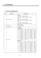
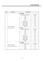
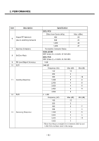
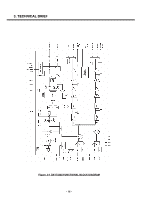
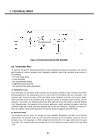
3. TECHNICAL BRIEF 3. TECHNICAL BRIEF 3.1 Power Transceiver (SKY74400, U501) The RF parts consist of a transmitter part, a receiver part, a frequency synthesizer part, a voltage supply part, and a VCTCXO part. The SKY74400 power transceiver is a highly integrated device for quad-band Global System for Mobile Communications (GSM), General Packet Radio Service (GPRS), and Enhanced Data for GSM Evolution (EDGE) handsets. The device supports GSM850, EGSM900, DCS1800, and PCS1900 applications. The power transceiver consists of a direct conversion receiver and power amplifier (PA) with an integrated PA Control (iPAC) function, fully integrated into a single module. All RF inputs and outputs of the device are fully matched to 50 . The receiver path implements a direct down-conversion architecture that eliminates the need for Intermediate Frequency(IF) components. Four integrated Low Noise Amplifiers (LNAs) are internally matched to 50 , which eliminates the need for external matching components. The receiver path also contains a quadrature demodulator, selectable receiver baseband filter bandwidths, low droop DCoffset correction sequencer, and integrated 2nd order Intercept Point (IP2) calibration circuitry. The SKY74400 also features an integrated, fully programmable, sigma-delta fractional-N synthesizer suitable for EGPRS multi-slot operation. The reference frequency for the synthesizer is supplied by an integrated Voltage Controlled Crystal Oscillator (VCXO) circuit that enables the use of a low-cost crystal. The VCXO also provides a buffered output to supply other devices in the system. The transmit path uses a translation loop architecture. This architecture consists of an In-phase and Quadrature (I/Q) modulator and a frequency translation loop to perform frequency up-conversion with high spectral purity. The translation loop also contains a phase-frequency detector, charge pump, mixer, programmable dividers, and high power transmit Voltage Controlled Oscillators (VCOs) with no external tank required. The transmit loop is directly connected to the PA section of the power transceiver, which consists of separate GSM850/EGSM900 and DCS1800/PCS1900 blocks fabricated on a single GaAs Heterojunction Bipolar Transistor (HBT) die, impedance matching circuitry for 50 output, and a custom BiCMOS PA control block with an internal current-sense resistor. • Receive section. Includes four integrated LNAs with 50 Ω inputs, quadrature demodulator circuitry that performs direct down-conversion, baseband amplifier circuitry with I/Q outputs, baseband filter with programmable bandwidths, five stages of DC offset correction, and IP2 calibration circuitry. • Synthesizer section. Includes an integrated VCO locked by a fractional-N synthesizer loop, a crystal oscillator to supply the reference frequency, a reference frequency output buffer, and an integrated loop filter. • Transmit section. The transmit section is designed with a translation loop architecture that consists of an I/Q modulator, integrated high power VCOs, offset mixer, programmable divider, Phase/Frequency Detector (PFD), charge pump, and loop filter. The transmit section also includes a PA for GSM850/EGSM900 and DCS1800/PCS1900 operation with common power supply pins, 50Ω output impedance matching circuitry, and a Power Amplifier Controller (PAC) block with an internal current-sense resistor. - 15 -
-
 1
1 -
2
-
3
-
4
-
5
-
6
-
7
-
8
-
 9
9 -
 10
10 -
 11
11 -
 12
12 -
 13
13 -
 14
14 -
 15
15 -
 16
16 -
 17
17 -
 18
18 -
 19
19 -
20
-
21
-
22
-
23
-
24
-
25
-
26
-
27
-
28
-
29
-
30
-
31
-
32
-
33
-
34
-
35
-
36
-
37
-
38
-
39
-
40
-
41
-
42
-
43
-
44
-
45
-
46
-
47
-
48
-
49
-
50
-
51
-
52
-
53
-
54
-
55
-
56
-
57
-
58
-
59
-
60
-
61
-
62
-
63
-
64
-
65
-
66
-
67
-
68
-
69
-
70
-
71
-
72
-
73
-
74
-
75
-
76
-
77
-
78
-
79
-
80
-
81
-
82
-
83
-
84
-
85
-
86
-
87
-
88
-
89
-
90
-
91
-
92
-
93
-
94
-
95
-
96
-
97
-
98
-
99
-
100
-
101
-
102
-
103
-
104
-
105
-
106
-
107
-
108
-
109
-
110
-
111
-
112
-
113
-
114
-
115
-
116
-
117
-
118
-
119
-
120
-
121
-
122
-
123
-
124
-
125
-
126
-
127
-
128
-
129
-
130
-
131
-
132
-
133
-
134
-
135
-
136
-
137
-
138
-
139
-
140
-
141
-
142
-
143
-
144
-
145
-
146
-
147
-
148
-
149
-
150
-
151
-
152
-
153
-
154
-
155
-
156
-
157
-
158
-
159
-
160
 |
 |