LG M6100 Service Manual - Page 24
Control Processor Subsystem, DSP Subsystem, Encoding/Decoding Algorithms, Peripheral Subsystem,
 |
View all LG M6100 manuals
Add to My Manuals
Save this manual to your list of manuals |
Page 24 highlights
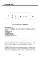
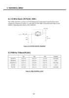
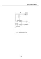
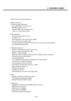
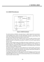
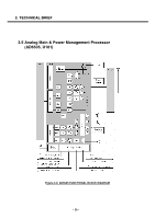
3. TECHNICAL BRIEF • AD6527 is an ADI designed processor. • AD6527 consists of 1. Control Processor Subsystem • 32-bit ARM7TDMI Control Processor • 58.5 MHz operation at 1.7V • On-board 16KB instruction/Data Cache • 1 Mbits of on-chip System SRAM 2. DSP Subsystem • 16-bit Fixed Point DSP Processor • 91 MIPS at 1.7V • 16K word Data and 16K word Program SRAM • 4K word Program Instruction Cache • Architecture supports Full Rate, Enhanced Full Rate, Half Rate, and AMR Speech Encoding/Decoding Algorithms 3. Peripheral Subsystem • Shared on-chip peripheral and off-chip interface: • Support for Burst and Page Mode Flash • Support for Pseudo SRAM • Ciphering module for GPRS supporting GAE1 and GAE2 encryption algorithms • Parallel and Serial Display Interface • 8 x 8 Keypad Interface • Four independent programmable backlight plus One Service Light • 1.8V and 3.0V, 64 kbps SIM interface • Universal System Connector Interface • Slow, Medium and Fast IrDA transceiver interface • Enhanced Generic Serial Port • Dedicated SPI interface • Thumbwheel Interface • JTAG Interface for Test and In-Circuit Emulation 4. Other • Supports 13 MHz and 26 MHz Input Clocks • 1.8V Typical Core Operating Voltages • 204-Ball LFBGA(mini-BGA) Package 5. Applications • GSM900/DCS1800/PCS1900/PCS850 Wireless Terminals • GSM Phase 2+ Compliant • GPRS Class 12 Compliant • Multimedia Services(MMS) • Extended Messaging System(EMS) - 25 -
-
 1
1 -
2
-
3
-
4
-
5
-
6
-
7
-
8
-
9
-
10
-
11
-
12
-
13
-
14
-
15
-
16
-
17
-
18
-
 19
19 -
 20
20 -
 21
21 -
 22
22 -
 23
23 -
 24
24 -
 25
25 -
 26
26 -
 27
27 -
 28
28 -
 29
29 -
30
-
31
-
32
-
33
-
34
-
35
-
36
-
37
-
38
-
39
-
40
-
41
-
42
-
43
-
44
-
45
-
46
-
47
-
48
-
49
-
50
-
51
-
52
-
53
-
54
-
55
-
56
-
57
-
58
-
59
-
60
-
61
-
62
-
63
-
64
-
65
-
66
-
67
-
68
-
69
-
70
-
71
-
72
-
73
-
74
-
75
-
76
-
77
-
78
-
79
-
80
-
81
-
82
-
83
-
84
-
85
-
86
-
87
-
88
-
89
-
90
-
91
-
92
-
93
-
94
-
95
-
96
-
97
-
98
-
99
-
100
-
101
-
102
-
103
-
104
-
105
-
106
-
107
-
108
-
109
-
110
-
111
-
112
-
113
-
114
-
115
-
116
-
117
-
118
-
119
-
120
-
121
-
122
-
123
-
124
-
125
-
126
-
127
-
128
-
129
-
130
-
131
-
132
-
133
-
134
-
135
-
136
-
137
-
138
-
139
-
140
-
141
-
142
-
143
-
144
-
145
-
146
-
147
-
148
-
149
-
150
-
151
-
152
-
153
-
154
-
155
-
156
-
157
-
158
-
159
-
160
 |
 |