LG M6100 Service Manual - Page 16
Receiver Part
 |
View all LG M6100 manuals
Add to My Manuals
Save this manual to your list of manuals |
Page 16 highlights
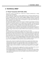
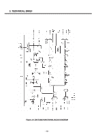
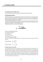
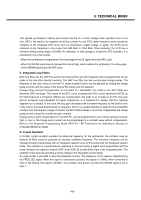
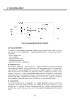
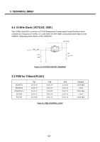
3. TECHNICAL BRIEF (1) Receiver Part A. LNA and Quadrature Demodulator Four separate LNAs are integrated in the SKY74400 to address different bands of operation. These LNAs have separate singleended 50 inputs. The LNA gain is switchable between high and low settings using the three-wire bus. The LNA outputs feed into a quadrature demodulator that downconverts the RF signals directly to baseband. The baseband I and Q paths consist of cascaded amplifiers and low pass filter sections. The baseband section provides eight programmable bandwidth settings ranging between 90 kHz and 160 kHz to allow for added flexibility when interfacing to any mixed signal baseband device. No external capacitors are required for baseband filtering. The filter chain consists of two fixed real poles, two fixed conjugate pole pairs, and one programmable conjugate pole pair. The result is a flat passband with minimal group delay distortion at any bandwidth setting. B. DC Offset Correction Five DC offset correction loops ensure that DC offsets generated in the SKY74400 do not overload the baseband chain at any point. After correction, the corrected voltages are held digitally for the duration of the receive slot(s). The positive edge of the RXENA signal starts the digital DC offset correction. Since the correction is digital, a system clock is required. To generate the clock, the reference frequency is divided down internally. A special, fast DC offset correction is carried out every time the receiver gain is programmed while RXENA is high. This ensures that a DC offset correction is complete in the time available, even if the gain is changed between slots in multislot mode. C. AM Suppression and IP2 Calibration For direct conversion GSM applications, it is imperative to have extremely low second-order distortion. Mathematically, secondorder distortion of a constant tone generates a DC term proportional to the square of the amplitude. In general, a strong interfering Amplitude Modulated (AM) signal is, therefore, demodulated by second-order distortion, which generates an Acinterfering baseband signal. The SKY74400 can effectively handle such AM-modulated interferers. A commonly used measure for receiver second-order distortion is the second-order intercept point, IP2. For example, to ensure that the unwanted baseband signals are 9 dB below the wanted signal required under the AM suppression test for type approval (see 3GPP TS 51.010-1), an input IP2 of 43 dBm is required. The SKY74400 RF transceiver includes a circuit that minimizes second-order distortion. This IP2 calibration circuit effectively compensates for any secondorder distortion in the receive chain that would otherwise generate unwanted baseband signals in the presence of strong interfering signals. When calibrated correctly, the SKY74400 IP2 meets the GSM AM suppression test requirements in all bands with good margin. A one-time factory calibration procedure produces a set of I/Q compensation coefficients that are programmed in the device to minimize the DC voltage shift resulting from the second-order distortion. The IP2 performance is optimized when the DC due to the interfering signal is minimized. The determined coefficients are transmitted to the serial interface, stored in nonvolatile memory, and programmed to the SKY74400 upon each power-up as part of device initialization. The optimization process is performed internal to the SKY74400. - 17 -
-
 1
1 -
2
-
3
-
4
-
5
-
6
-
7
-
8
-
9
-
10
-
 11
11 -
 12
12 -
 13
13 -
 14
14 -
 15
15 -
 16
16 -
 17
17 -
 18
18 -
 19
19 -
 20
20 -
 21
21 -
22
-
23
-
24
-
25
-
26
-
27
-
28
-
29
-
30
-
31
-
32
-
33
-
34
-
35
-
36
-
37
-
38
-
39
-
40
-
41
-
42
-
43
-
44
-
45
-
46
-
47
-
48
-
49
-
50
-
51
-
52
-
53
-
54
-
55
-
56
-
57
-
58
-
59
-
60
-
61
-
62
-
63
-
64
-
65
-
66
-
67
-
68
-
69
-
70
-
71
-
72
-
73
-
74
-
75
-
76
-
77
-
78
-
79
-
80
-
81
-
82
-
83
-
84
-
85
-
86
-
87
-
88
-
89
-
90
-
91
-
92
-
93
-
94
-
95
-
96
-
97
-
98
-
99
-
100
-
101
-
102
-
103
-
104
-
105
-
106
-
107
-
108
-
109
-
110
-
111
-
112
-
113
-
114
-
115
-
116
-
117
-
118
-
119
-
120
-
121
-
122
-
123
-
124
-
125
-
126
-
127
-
128
-
129
-
130
-
131
-
132
-
133
-
134
-
135
-
136
-
137
-
138
-
139
-
140
-
141
-
142
-
143
-
144
-
145
-
146
-
147
-
148
-
149
-
150
-
151
-
152
-
153
-
154
-
155
-
156
-
157
-
158
-
159
-
160
 |
 |