Oki C7200 Service Manual - Page 23
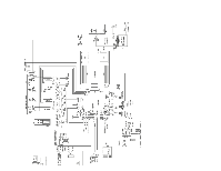
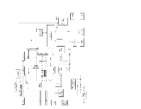
panel I/F, IDE I/F, Centronics I/F, USB I/F, PCI I/F, EEPROM and a SPD SDRAM DIMM
 |
View all Oki C7200 manuals
Add to My Manuals
Save this manual to your list of manuals |
Page 23 highlights
(1) CPU The CPU is PowerPC750, a 64-bit bus RISC processor, which inputs an 80-MHz CLK (=BUS CLK), and operates at 400MHz that is five times the input. (2) Secondary Cache SRAM SRAM is included as secondary cache of the CPU on the board. (3) ROM ROM is to be inserted into the three 168 pin DIMM slots. The slot A is for program ROM and the slot B is for Japanese kanji fonts. The slot C is not assigned. (4) RAM RAM is to be inserted into the four 168 pin DIMM slots. The DIMMs must be fitted in descending labeled type No. order into the slots 1, 3, 2 and 4. SDRAM DIMM Specifications: Speed: PC100 or more Capacity: 64/128/256 MB Configuration: Without parity. Without ECC. SPD information is required. Number of chips contained = 8 or 16. (5) EEPROM EEPROM, an 8-pin DIP package, is to be inserted into the IC socket. The EEPROM is of 16 Kbits for 3.3V power supply, and settings for controlling the controller block are stored in it. (6) Flash ROM A 2-Mbyte flash ROM is surface-mounted on the CRM board. The flash ROM is composed of four 256-k-by-16bit chips, and fonts and macros can be stored in it. (7) Memory control LSI (CI) A 696-pin BGA package ASIC made by NEC, which is equipped with a cooling heat sink and mainly controls a CPU I/F, memory, video data compression and decompression, and a PU-video I/F. (8) Interface control LSI (C2) A BGA package ASIC made by Toshiba, which controls a PU command I/F, operator panel I/F, IDE I/F, Centronics I/F, USB I/F, PCI I/F, EEPROM and a SPD (SDRAM DIMM) I/F. (9) IDE HDD An IDE connector is surface-mounted on the board to which an IDE HDD assembled using
-
 1
1 -
2
-
3
-
4
-
5
-
6
-
7
-
8
-
9
-
10
-
11
-
12
-
13
-
14
-
15
-
16
-
17
-
 18
18 -
 19
19 -
 20
20 -
 21
21 -
 22
22 -
 23
23 -
 24
24 -
 25
25 -
 26
26 -
 27
27 -
 28
28 -
29
-
30
-
31
-
32
-
33
-
34
-
35
-
36
-
37
-
38
-
39
-
40
-
41
-
42
-
43
-
44
-
45
-
46
-
47
-
48
-
49
-
50
-
51
-
52
-
53
-
54
-
55
-
56
-
57
-
58
-
59
-
60
-
61
-
62
-
63
-
64
-
65
-
66
-
67
-
68
-
69
-
70
-
71
-
72
-
73
-
74
-
75
-
76
-
77
-
78
-
79
-
80
-
81
-
82
-
83
-
84
-
85
-
86
-
87
-
88
-
89
-
90
-
91
-
92
-
93
-
94
-
95
-
96
-
97
-
98
-
99
-
100
-
101
-
102
-
103
-
104
-
105
-
106
-
107
-
108
-
109
-
110
-
111
-
112
-
113
-
114
-
115
-
116
-
117
-
118
-
119
-
120
-
121
-
122
-
123
-
124
-
125
-
126
-
127
-
128
-
129
-
130
-
131
-
132
-
133
-
134
-
135
-
136
-
137
-
138
-
139
-
140
-
141
-
142
-
143
-
144
-
145
-
146
-
147
-
148
-
149
-
150
-
151
-
152
-
153
-
154
-
155
-
156
-
157
-
158
-
159
-
160
-
161
-
162
-
163
-
164
-
165
-
166
-
167
-
168
-
169
-
170
-
171
-
172
-
173
-
174
-
175
-
176
-
177
-
178
-
179
-
180
-
181
-
182
-
183
-
184
-
185
-
186
-
187
-
188
-
189
-
190
-
191
-
192
-
193
-
194
-
195
-
196
-
197
-
198
-
199
-
200
-
201
-
202
-
203
-
204
-
205
-
206
-
207
-
208
-
209
-
210
-
211
-
212
-
213
-
214
-
215
-
216
-
217
-
218
-
219
-
220
-
221
-
222
-
223
-
224
-
225
-
226
-
227
-
228
-
229
-
230
-
231
-
232
-
233
-
234
-
235
-
236
-
237
-
238
-
239
-
240
-
241
-
242
-
243
-
244
-
245
-
246
-
247
-
248
-
249
-
250
-
251
-
252
-
253
-
254
-
255
-
256
-
257
-
258
-
259
-
260
-
261
-
262
-
263
-
264
-
265
-
266
-
267
-
268
-
269
-
270
-
271
-
272
-
273
-
274
-
275
-
276
-
277
-
278
-
279
-
280
-
281
-
282
-
283
-
284
-
285
-
286
-
287
-
288
-
289
-
290
-
291
-
292
-
293
-
294
-
295
-
296
-
297
-
298
-
299
-
300
-
301
-
302
-
303
-
304
-
305
-
306
-
307
-
308
-
309
-
310
-
311
-
312
-
313
-
314
-
315
-
316
-
317
-
318
-
319
-
320
-
321
-
322
-
323
-
324
-
325
-
326
-
327
-
328
-
329
-
330
-
331
-
332
-
333
-
334
-
335
-
336
-
337
-
338
-
339
-
340
-
341
-
342
-
343
-
344
-
345
-
346
-
347
-
348
-
349
-
350
-
351
-
352
-
353
-
354
-
355
-
356
-
357
-
358
-
359
-
360
-
361
-
362
-
363
-
364
-
365
-
366
-
367
-
368
-
369
-
370
-
371
-
372
-
373
-
374
-
375
-
376
-
377
-
378
-
379
-
380
-
381
-
382
-
383
-
384
-
385
-
386
-
387
-
388
-
389
-
390
-
391
 |
 |
