Sharp ER-A450T Service Manual - Page 24
Clock generator, Reset POFF circuit - memory
 |
View all Sharp ER-A450T manuals
Add to My Manuals
Save this manual to your list of manuals |
Page 24 highlights
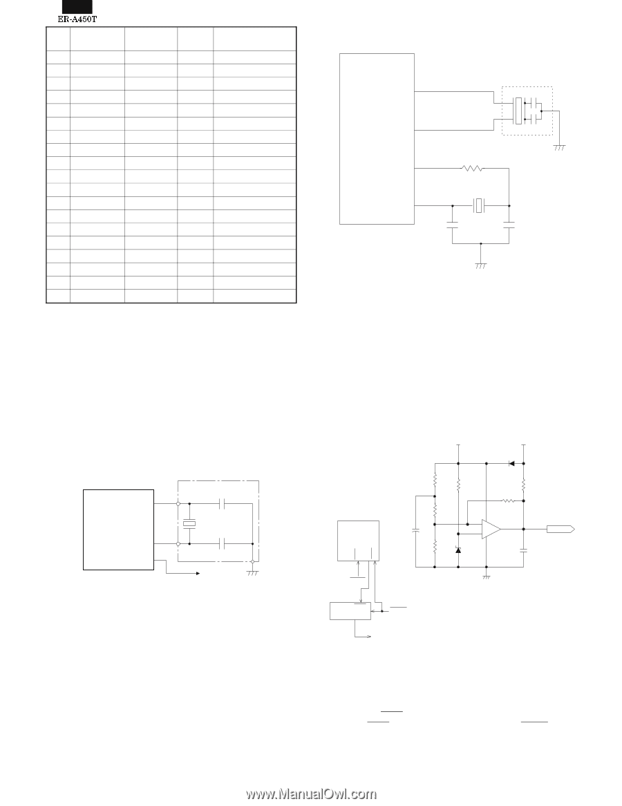
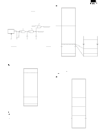
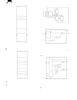
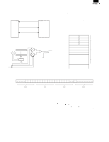
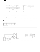
Pin NO. 142 143 144 145 146 147 148 149 150 151 152 153 154 155 156 157 158 159 160 I ID IS ISU IO 3S ON6 Name ER-A770 I/O VCC VCC GND GND /CSD VCC IS TRNDTD NC O /DTRD NC O /RTSD NC O RCVDTD GND IS /CTSD GND IS /DSRD GND IS TRNRDYD NC O RCVRDYD NC O TRNEMPD NC O SYCBKD NC IO /WIN /WRH I /RIN /RDH I RSLCT0 AH0 I RSLCT1 AH1 I RST RES USART IS MCLK CLK USART I TTL input TTL input with pull down TTL Schmidt input TTL Schmidt input with pull up TTL I/O 3-state Buffer (6mA) Open drain (6mA) Description +5V GND +5V NC NC NC GND GND GND NC NC NC NC Write signal Read signal Address bus Address bus Reset signal Clock (4.91MHz) 3. Clock generator 1) CPU (HD64151010FX) XTAL 99 CPU (HD64151010FX) EXTAL 98 101 X4 19.66MHz PHAI Fig. 3-1 Basic clock is supplied from a 19.66 MHz ceramic oscillator. The CPU contains an oscillation circuit from which the basic clock is internally driven. If the CPU was not operating properly, the signal does not appear on this line in most cases. 2) CKDC8 oscillation circuit 40 X2 CKDC 8 41 X1 37 XT2 38 XT1 HD404728A91FS C106 18P X1 4.19MHz 1 2 3 R164 330K X2 32.768KHz C105 33P Fig. 3-2 Two oscillators are connected to the CKDC8. The main clock X1 generates 4.19MHz which is used during power on. When power is turned off, the CKDC8 goes into the standby mode and the main clock stops. The sub-clock X2 generates 32.768KHz which is primarily used to update the internal RTC (real time clock). During the standby mode, it keeps oscillating to update the clock and monitoring the power recovery. 4. Reset (POFF) circuit +24V +5V INT0 IRQ0 MPCA7 13 54 48 POFF D7 R114 8.2KG + C83 1µ 50V R115 15KG R116 9.1KG 1SS133 R117 2.7K R118 R119 2.7K 56K 8 3+ B 1 2 - IC7A 4 KIA393F ZD2 MTZ5.1A /POFF C37 1000P 89 IRQ0 1 CPU 72 RESET (FROM CKDC 8) STOP (TO CKDC 8) Fig. 4-1 In order to prevent memory loss at a time of power off and power supply failure of the ECR, the power supply condition is monitored at all times. When a power failure is met, the CPU suspends the execution of the current program and immediately executes the power-off program to save the data in the CPU registers in the external S-RAM with the signal STOP forced low to prepare for the power-off situation. The signal STOP is supplied to the CKDC8 as signal RESET to reset the devices. This circuit monitors +24V supply voltage. 4 - 16
-
 1
1 -
2
-
3
-
4
-
5
-
6
-
7
-
8
-
9
-
10
-
11
-
12
-
13
-
14
-
15
-
16
-
17
-
18
-
 19
19 -
 20
20 -
 21
21 -
 22
22 -
 23
23 -
 24
24 -
 25
25 -
 26
26 -
 27
27 -
 28
28 -
 29
29 -
30
-
31
-
32
-
33
-
34
-
35
-
36
-
37
-
38
-
39
-
40
-
41
-
42
-
43
-
44
-
45
-
46
-
47
-
48
-
49
-
50
-
51
-
52
-
53
-
54
-
55
-
56
-
57
-
58
-
59
-
60
-
61
-
62
-
63
-
64
-
65
-
66
-
67
-
68
-
69
-
70
-
71
-
72
-
73
-
74
-
75
-
76
 |
 |