Sharp ER-A450T Service Manual - Page 28
PRINTER control circuit
 |
View all Sharp ER-A450T manuals
Add to My Manuals
Save this manual to your list of manuals |
Page 28 highlights
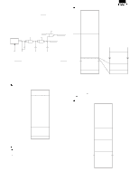
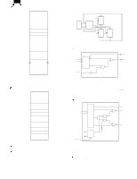
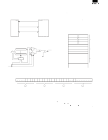
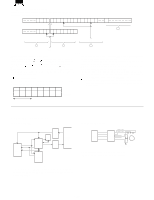
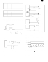
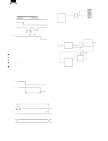
3) SSP register access method Access to SSP break address register is performed through the temporary register as shown below: A19 A18 A17 A16 A15 A8 A7 Temporary Temporary A2 EN 4 WR 1 2 3 WR Fig. 6-5 Enable flags can be accessed individually. Though enable register can be accessed individually, writing to break address registers and is performed at the same time as writing to break address register through the temporary register. Therefore, set and to temporary, then write into last. Since the temporary register is commonly used by BAR sets, the following register setting is performed after completion of setting of each break address register. SSP control method Access to the enable register and the break address register is only possible when writing to them from the CPU. Information on which break register the SSP break is detected and is read as binary data by reading address FFFFFFH (*1). If there are 32 break registers, the binary expression is made with the above 5 bits, and 0th is "00000B" and 31st is "11111B." When detected simultaneously by two or more break registers, one with the smaller BAR number is read as binary data. The break signals (NMI) and the above detection data (CMP0~4) are held until the above detection data are read. Thus, the reading is made in the NMI sub routine. (Clear by FFFFFFH read.) 1: FFFFFFH is not fully decoded. (FFFF00H~FFFFFFH). Therefore any unnecessary read access in parentheses should not be performed. bit 7 6 5 4 3 2 1 0 0 0 0 CMP4 CMP3 CMP2 CMP1 CMP0 (FFFFFFH) 7. PRINTER control circuit 1) Block diagram RECEIVER CPU Address bus Data bus TPRC1 P.BRAM MPCA7 DRIVER PRINTER (PR-45) Fig. 7-1 • The thermal printer (PR-45M) is controlled by the thermal printer controller (TPRC1). The PB-RAM connected to TPRC1 serves as a print data buffer. 2) Paper feed circuit TPRC1 RAS/JAS RBS/JBS RCS/JCS RDS/JDS RPFA/JPFA RPFB/JPFB 4AC16 RPFC/JPFC RPPD/JPFD BA C M D VRCOM/VJCOM • A pulse motor is used as the paper feed motor. • Drive sequence of the pulse motor is as follows: 4 - 20
-
 1
1 -
2
-
3
-
4
-
5
-
6
-
7
-
8
-
9
-
10
-
11
-
12
-
13
-
14
-
15
-
16
-
17
-
18
-
19
-
20
-
21
-
22
-
 23
23 -
 24
24 -
 25
25 -
 26
26 -
 27
27 -
 28
28 -
 29
29 -
 30
30 -
 31
31 -
 32
32 -
 33
33 -
34
-
35
-
36
-
37
-
38
-
39
-
40
-
41
-
42
-
43
-
44
-
45
-
46
-
47
-
48
-
49
-
50
-
51
-
52
-
53
-
54
-
55
-
56
-
57
-
58
-
59
-
60
-
61
-
62
-
63
-
64
-
65
-
66
-
67
-
68
-
69
-
70
-
71
-
72
-
73
-
74
-
75
-
76
 |
 |