Sharp ER-A450T Service Manual - Page 26
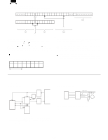
RAM area memory map, I/O area memory map, ROM control, RAM control
 |
View all Sharp ER-A450T manuals
Add to My Manuals
Save this manual to your list of manuals |
Page 26 highlights
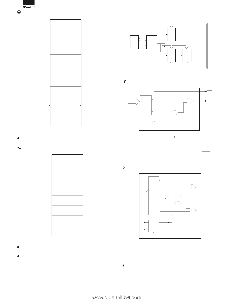
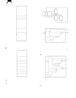
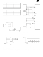
RAM area memory map 100000H NOT USE 1C0000H 1E0000H 200000H RAS1 128K Byte RAS2 128K Byte 280000H 400000H RAS3 512K Byte (OPTION) (MAX 2MB) NOT USE BFFFFFH Fig. 5-4 Note: RAS2 signal is formed as OR in the image area of 0 page. (lower32KB). I/O area memory map 00FF80H (*1) MPCCS 00FFA0H NOT USE 00FFC0H 00FFD0H 00FFE0H 00FFE8H 00FFF0H 00FFFFH MCR1 (NOT USE) MCR2 (NOT USE) (*2) OPCCS1 (*2) OPCCS2 NOT USE NOT USE NOT USE Fig. 5-5 Note 1: MPCCS signal is the base signal for MPCA7 internal register decoding, and does not exist as an internal signal. Note 2: OPCCS1 and OPCCS2 signals are decoded in the OPC (optionperipheral controller) using the base signal OPTCS for option decoding. They does not exist as external signals. 2) Block diagram Data bus CPU ROS1 ROM1 MPCA6 Address bus RAM1 RAM2 RAS2 RAS3 (OPTION) ROM control Fig. 5-6 Address A23~A14 C80000H~CFFFFFH C00000H~C7FFFFH Address decorder 000000H~007FFFH ROS2 ROS1 (IPLON) MPCA7 Fig. 5-7 IPLON: IPL board detection signal incorporated in the option slot. Note used in the ER-A445P. (Not used) Access is performed with two ROM chip select signals ROS1 and ROS2, which decode 512KB address area respectively to accessmax. 4MB ROM. RAM control Address A23~A14 200000H~3FFFFFH 1C0000H~1DFFFFH Address decorder 008000H~ 00F7FFH *1 1E0000H~1FFFFFH RAS3 RAS1 RAS2 DOI D Q Control register S8F CK R RESET MPCA7 Fig. 5-8 Access is performed with two RAM chip select signals, RAS2 and RAS3. The control register in MPCA7 allows selection of page image memory area. (RAS1 is selected for initializing.) : For 0 page image area, selection between RAS2 and RAS3 can bemade with the control register. The 0 page control register performs initializing at the timing of no stack process immediately after resetting. 4 - 18
-
 1
1 -
2
-
3
-
4
-
5
-
6
-
7
-
8
-
9
-
10
-
11
-
12
-
13
-
14
-
15
-
16
-
17
-
18
-
19
-
20
-
 21
21 -
 22
22 -
 23
23 -
 24
24 -
 25
25 -
 26
26 -
 27
27 -
 28
28 -
 29
29 -
 30
30 -
 31
31 -
32
-
33
-
34
-
35
-
36
-
37
-
38
-
39
-
40
-
41
-
42
-
43
-
44
-
45
-
46
-
47
-
48
-
49
-
50
-
51
-
52
-
53
-
54
-
55
-
56
-
57
-
58
-
59
-
60
-
61
-
62
-
63
-
64
-
65
-
66
-
67
-
68
-
69
-
70
-
71
-
72
-
73
-
74
-
75
-
76
 |
 |