Sharp ER-A450T Service Manual - Page 27
SSP circuit - service
 |
View all Sharp ER-A450T manuals
Add to My Manuals
Save this manual to your list of manuals |
Page 27 highlights
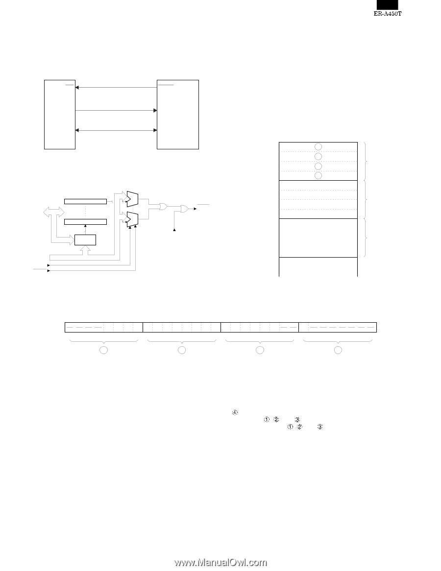
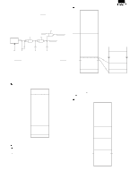
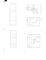
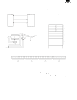
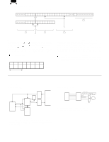
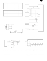
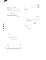
6. SSP circuit 1) Block diagram This is the circuit employed for implementing the Special Service Preset(SSP). (Block diagram) NMI SSPRQ As the address detection system, the break address register comparison system is employed though the mapping system and employed in the conventional monitor RAM. The address register located in MPCA is always compared with the system address bus to monitor and generate the NMI signal at a synchronized timing and to go to the NMI exception process. In the exception process routine of the service routine, the entry address is checked to go to the SSP sub routine. Entry to the break address register (BAR) is performed through the address FFFF00H or later decoded in MPCA7. A0~23 D0~D7 CPU (MPCA7 block diagram) D0~ D7 BAR 0 BAR N REGCS Decode Fig. 6-1 MPCA7 Comparator O Coincide N Coincide SSPRQ (NMI) SPE (Enable register) 2) SSP register The break address register (BAR) is accessed through the direct address of FFFF00H~FFFFFFH. Entry number is 32 entry. FFFF00 7 0 H 1 1 2 2 3 BAR0 3 4 4 5 BAR1 6 7 BAR2 A23~ A0 Control signal ROMCS Fig. 6-2 A19 A18 A17 A16 A15 Fig. 6-3 Each BAR is composed of 4 a byte address. The bit composition is as follows: A8 A7 A2 EN 1 Upper bits 2 Intermediate bits Don't care for "-----." 3 Lower bits 4 Enable register EN (bit7) = 1 Enable = 0 Inhibit < BAR composition > Fig. 6-4 is the enable register. The entry registers of the break address are assigned to , , and . Each bit of address corresponds to each bit position, writing to , , and is performed without shifting. The corresponding area is the 1MB space of ROS1 and ROS2. 4 - 19
-
 1
1 -
2
-
3
-
4
-
5
-
6
-
7
-
8
-
9
-
10
-
11
-
12
-
13
-
14
-
15
-
16
-
17
-
18
-
19
-
20
-
21
-
 22
22 -
 23
23 -
 24
24 -
 25
25 -
 26
26 -
 27
27 -
 28
28 -
 29
29 -
 30
30 -
 31
31 -
 32
32 -
33
-
34
-
35
-
36
-
37
-
38
-
39
-
40
-
41
-
42
-
43
-
44
-
45
-
46
-
47
-
48
-
49
-
50
-
51
-
52
-
53
-
54
-
55
-
56
-
57
-
58
-
59
-
60
-
61
-
62
-
63
-
64
-
65
-
66
-
67
-
68
-
69
-
70
-
71
-
72
-
73
-
74
-
75
-
76
 |
 |