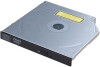
TEAC DW-224E-V Hardware Specification - Page 14
Ide Hardware Interface - ata
 |
View all TEAC DW-224E-V manuals
Add to My Manuals
Save this manual to your list of manuals |
Page 14 highlights
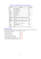
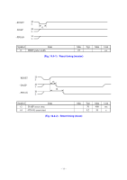
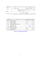
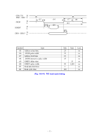
14. IDE HARDWARE INTERFACE 14.1 Outline (1) Applicable standard ANSI standard SFFC : X3T13/1321D (ATA-5) : SFF-8020i Rev. 2.6 and SFF-8090v3 14.2 Electrical Characteristics The following specifications apply to the interface connector terminal for the IDE signal of the drive. The input signals refer to the signals input to the drive whereas the output signals refer to the signals output from the drive. (1) Tri-state input/output signals (DD0 to DD15, -PDIAG) (a) Input signal level • Low level : 0 to 0.8VDC • High level : 2.0 to 5.25VDC • Hysteresis : possessed • Maximum input current : ±25µA (b) Output signal level • Low level : 0 to 0.4VDC (output sink current 12mA) • High level : 2.7 to 3.3VDC (output source current 1mA) • Maximum output current at high impedance : ±25µA (c) Termination (DD0 to DD15) • Pull-up resistance : Not equipped • Series resistance : 33Ω (d) Termination (-PDIAG) • Pull-up resistance : 10kΩ • Series resistance : 0Ω (2) Open drain input/output signals (-DASP) (a) Input signal level • Low level : 0 to 0.8VDC • High level : 2.0 to 5.25VDC • Hysteresis : possessed • Maximum input current : ±25µA (excluding the pull-up resistance) (b) Output signal level • Low level : 0 to 0.4VDC (output sink current 12mA) • Maximum output current at high impedance : ±25µA (c) Termination • Pull-up resistance : 10kΩ • Series resistance : 0Ω (3) Tri-state output signals (DMARQ, INTRQ, IORDY) • Low level : 0 to 0.4VDC (output sink current 12mA) • High level : 2.7 to 3.3VDC (output source current 1mA) • Maximum output current at high impedance : ±25µA • Series resistance : 22Ω - 12 -
-
 1
1 -
2
-
3
-
4
-
5
-
6
-
7
-
8
-
 9
9 -
 10
10 -
 11
11 -
 12
12 -
 13
13 -
 14
14 -
 15
15 -
 16
16 -
 17
17 -
 18
18 -
 19
19 -
20
-
21
-
22
-
23
-
24
-
25
-
26
-
27
-
28
-
29
-
30
-
31
-
32
-
33
-
34
 |
 |
