Asus P3V133 P3V133 User Manual - Page 56
Chip Configuration
 |
View all Asus P3V133 manuals
Add to My Manuals
Save this manual to your list of manuals |
Page 56 highlights
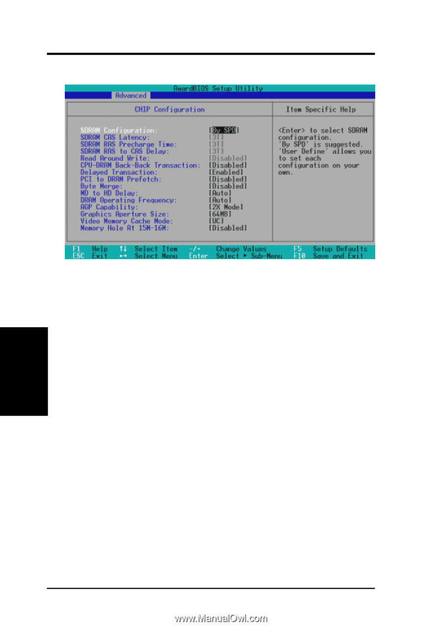
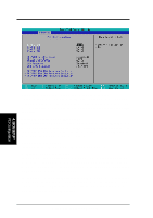
4. BIOS SETUP 4.4.1 Chip Configuration 4. BIOS SETUP Chip Configuration SDRAM Configuration [By SPD] This sets the optimal timings for items 2-5, depending on the memory modules that you are using. Default setting is [By SPD], which configures items 2-5 by reading the contents in the SPD (Serial Presence Detect) device. The EEPROM on the memory module stores critical parameter information about the module, such as memory type, size, speed, voltage interface, and module banks. Configuration options: [User Define] [7ns (143MHz)] [8ns (125MHz)] [By SPD] SDRAM CAS Latency This controls the latency between the SDRAM read command and the time that the data actually becomes available. NOTE: To make changes to this field, the SDRAM Configuration field must be set to [User Define]. SDRAM RAS Precharge Time This controls the idle clocks after issuing a precharge command to the SDRAM. NOTE: To make changes to this field, the SDRAM Configuration field must be set to [User Define]. SDRAM RAS to CAS Delay This controls the latency between the SDRAM active command and the read/write command. NOTE: To make changes to this field, the SDRAM Configuration field must be set to [User Define]. Read Around Write With the Read Around Write (RAW) feature, after the CPU issues a write command, the memory controller stores the write data in its buffer so that next time the CPU needs the data, it can provide them without accessing the SDRAM. NOTE: To make changes to this field, the SDRAM Configuration field must be set to [User Define]. 56 ASUS P3V133 User's Manual
-
 1
1 -
2
-
3
-
4
-
5
-
6
-
7
-
8
-
9
-
10
-
11
-
12
-
13
-
14
-
15
-
16
-
17
-
18
-
19
-
20
-
21
-
22
-
23
-
24
-
25
-
26
-
27
-
28
-
29
-
30
-
31
-
32
-
33
-
34
-
35
-
36
-
37
-
38
-
39
-
40
-
41
-
42
-
43
-
44
-
45
-
46
-
47
-
48
-
49
-
50
-
 51
51 -
 52
52 -
 53
53 -
 54
54 -
 55
55 -
 56
56 -
 57
57 -
 58
58 -
 59
59 -
 60
60 -
 61
61 -
62
-
63
-
64
-
65
-
66
-
67
-
68
-
69
-
70
-
71
-
72
-
73
-
74
-
75
-
76
-
77
-
78
-
79
-
80
-
81
-
82
-
83
-
84
-
85
-
86
-
87
-
88
-
89
-
90
-
91
-
92
-
93
-
94
-
95
-
96
 |
 |