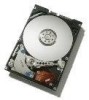
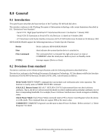
Hitachi HTS541010G9AT00 Specifications - Page 52
Signal definitions
 |
UPC - 000061425019
View all Hitachi HTS541010G9AT00 manuals
Add to My Manuals
Save this manual to your list of manuals |
Page 52 highlights
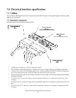
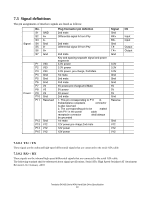
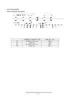
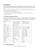
7.3 Signal definitions The pin assignments of interface signals are listed as follows: Signal Power No. S1 GND S2 A+ S3 AS4 Gnd S5 BS6 B+ S7 Gnd P1 V33 P2 V33 P3 V33 P4 Gnd P5 Gnd P6 Gnd P7 V5 P8 V5 P9 V5 P10 Gnd P11 Reserved P12 Gnd P13 V12 P14 V12 P15 V12 Plug Connector pin definition 2nd mate Differential signal A from Phy 2nd mate Differential signal B from Phy 2nd mate Key and spacing separate signal and power segments 3.3V power 3.3V power 3.3V power, pre-charge, 2nd Mate 1st mate 2nd mate 2nd mate 5V power,pre-charge,2nd Mate 5V power 5V power 2nd mate 1. This pin corresponding to P11 in thebackplane receptacle connector is also reserved 2. The corresponding pin to be mated with P11 in the power cable receptacle connector shall always be grounded 1st mate 12V power,pre-chage,2nd mate 12V power 12V power Signal Gnd RX+ RXGnd TXTX+ Gnd 3.3V 3.3V 3.3V Gnd Gnd Gnd 5V 5V 5V Gnd Reserve Gnd V12 V12 V12 I/O Input Input Output Output 7.3.0.1 TX+ / TX These signal are the outbound high-speed differrential signals that are connected to the serial ATA cable. 7.3.0.2 RX+ / RX These signals are the inbound high-speed differential signals that are connected to the serial ATA cable. The following standard shall be referenced about signal specifications. Serial ATA: High Speed Serialized AT Attachment Revision 1.0a 7-January -2003 Travelstar 5K100 (Serial ATA) Hard Disk Drive Specification 40
-
 1
1 -
2
-
3
-
4
-
5
-
6
-
7
-
8
-
9
-
10
-
11
-
12
-
13
-
14
-
15
-
16
-
17
-
18
-
19
-
20
-
21
-
22
-
23
-
24
-
25
-
26
-
27
-
28
-
29
-
30
-
31
-
32
-
33
-
34
-
35
-
36
-
37
-
38
-
39
-
40
-
41
-
42
-
43
-
44
-
45
-
46
-
 47
47 -
 48
48 -
 49
49 -
 50
50 -
 51
51 -
 52
52 -
 53
53 -
 54
54 -
 55
55 -
 56
56 -
 57
57 -
58
-
59
-
60
-
61
-
62
-
63
-
64
-
65
-
66
-
67
-
68
-
69
-
70
-
71
-
72
-
73
-
74
-
75
-
76
-
77
-
78
-
79
-
80
-
81
-
82
-
83
-
84
-
85
-
86
-
87
-
88
-
89
-
90
-
91
-
92
-
93
-
94
-
95
-
96
-
97
-
98
-
99
-
100
-
101
-
102
-
103
-
104
-
105
-
106
-
107
-
108
-
109
-
110
-
111
-
112
-
113
-
114
-
115
-
116
-
117
-
118
-
119
-
120
-
121
-
122
-
123
-
124
-
125
-
126
-
127
-
128
-
129
-
130
-
131
-
132
-
133
-
134
-
135
-
136
-
137
-
138
-
139
-
140
-
141
-
142
-
143
-
144
-
145
-
146
-
147
-
148
-
149
-
150
-
151
-
152
-
153
-
154
-
155
-
156
-
157
-
158
-
159
-
160
-
161
-
162
-
163
-
164
-
165
-
166
-
167
-
168
-
169
-
170
-
171
-
172
-
173
-
174
-
175
-
176
-
177
-
178
-
179
-
180
-
181
-
182
-
183
-
184
-
185
-
186
-
187
-
188
-
189
-
190
-
191
-
192
-
193
-
194
-
195
-
196
-
197
-
198
-
199
-
200
-
201
-
202
-
203
-
204
-
205
 |
 |
