Hitachi HTS541010G9AT00 Specifications - Page 58
Device Control Register, Device Register
 |
UPC - 000061425019
View all Hitachi HTS541010G9AT00 manuals
Add to My Manuals
Save this manual to your list of manuals |
Page 58 highlights
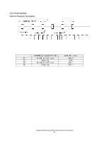
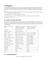
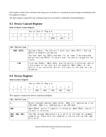
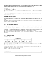
This register contains the command code being sent to the device. Command execution begins immediately after this register is written. All other registers required for the command must be set up before writing the Command Register. 9.3 Device Control Register Table 25: Device Control Register Device Control Register 7 6 5 4 3 2 1 0 - - - - 1 SRST -IEN 0 Bit Definitions SRST (RST) Software Reset. The device is held reset when RST=1. Setting RST=0 re-enables the device. The host must set RST=1 and wait for at least 5 microseconds before setting RST=0, to ensure that the device recognizes the resest. -IEN Interrupt Enable. When IEN=0, and the device is selected, device interurupts to the host will be enabled. When IEN=1, or the device is not selected, device interrupts to the host will be disabled. 9.4 Device Register Table 26: Device Register Device Control Register 7 6 5 4 3 2 1 0 1 L 1 DRV HS3 HS2 HS1 HS0 This register contains the device and head numbers. Bit Definitions L Binary encoded address mode select. When L=0, addressing is by CHS mode. When L=1, addressing is by LBA mode. DRV When DRV=0, device 0 (master) is selected. When DRV=1, device 1 (slave) is selected. HS3, HS2, HS1, HS0 The HS3 through HSO contain bits 24-27 of the LBA. At command completion, these bits are updated to reflect the current LBA bits 24-27. Travelstar 5K100 (Serial ATA) Hard Disk Drive Specification 46
-
 1
1 -
2
-
3
-
4
-
5
-
6
-
7
-
8
-
9
-
10
-
11
-
12
-
13
-
14
-
15
-
16
-
17
-
18
-
19
-
20
-
21
-
22
-
23
-
24
-
25
-
26
-
27
-
28
-
29
-
30
-
31
-
32
-
33
-
34
-
35
-
36
-
37
-
38
-
39
-
40
-
41
-
42
-
43
-
44
-
45
-
46
-
47
-
48
-
49
-
50
-
51
-
52
-
 53
53 -
 54
54 -
 55
55 -
 56
56 -
 57
57 -
 58
58 -
 59
59 -
 60
60 -
 61
61 -
 62
62 -
 63
63 -
64
-
65
-
66
-
67
-
68
-
69
-
70
-
71
-
72
-
73
-
74
-
75
-
76
-
77
-
78
-
79
-
80
-
81
-
82
-
83
-
84
-
85
-
86
-
87
-
88
-
89
-
90
-
91
-
92
-
93
-
94
-
95
-
96
-
97
-
98
-
99
-
100
-
101
-
102
-
103
-
104
-
105
-
106
-
107
-
108
-
109
-
110
-
111
-
112
-
113
-
114
-
115
-
116
-
117
-
118
-
119
-
120
-
121
-
122
-
123
-
124
-
125
-
126
-
127
-
128
-
129
-
130
-
131
-
132
-
133
-
134
-
135
-
136
-
137
-
138
-
139
-
140
-
141
-
142
-
143
-
144
-
145
-
146
-
147
-
148
-
149
-
150
-
151
-
152
-
153
-
154
-
155
-
156
-
157
-
158
-
159
-
160
-
161
-
162
-
163
-
164
-
165
-
166
-
167
-
168
-
169
-
170
-
171
-
172
-
173
-
174
-
175
-
176
-
177
-
178
-
179
-
180
-
181
-
182
-
183
-
184
-
185
-
186
-
187
-
188
-
189
-
190
-
191
-
192
-
193
-
194
-
195
-
196
-
197
-
198
-
199
-
200
-
201
-
202
-
203
-
204
-
205
 |
 |
